주요 콘텐츠

pcbStack

R2026b

Single feed or multi-feed PCB antenna

Description

The pcbStack object is a single-feed or multi-feed printed circuit board (PCB) antenna. Use the pcbStack object:

  • To create single-layer, multilayer metal, or metal-dielectric substrate antennas.

  • To create an arbitrary number of feeds and vias in an antenna.

  • To create a PCB antenna from antenna and array catalog elements.

Note

To generate a Gerber file, include a substrate layer. Use the Substrate property to create this layer in the PCB antenna. For more information, see Convert Circular Microstrip Patch into PCB Antenna.

Creation

Description

pcbant = pcbStack creates an air-filled single-feed PCB with two metal layers.

pcbant = pcbStack(PropertyName=Value) sets properties using one or more name-value arguments. PropertyName is the property name and Value is the corresponding value. For example, pcbStack(FeedDiameter=2e-04) creates a PCB antenna with a feed diameter of 0.2 mm. You can specify several name-value arguments in any order as PropertyName1=Value1,...,PropertyNameN=ValueN. Properties that you do not specify retain their default values.

example

pcbant = pcbStack(ant) converts any 2-D or 2.5-D antenna from the antenna catalog into a PCB antenna for modeling and analysis. You can also convert antenna array objects from the antenna array catalog to a PCB antenna. For a list of supported catalog elements, see Supported Catalog Elements.

example

Properties

expand all

Name of PCB antenna, specified as a string.

Example: "PCBPatch"

Data Types: string

Revision details of PCB antenna design, specified as a string.

Example: "2.0"

Data Types: string

Shape of the PCB board, specified as one of the following shape objects:

  • antenna.Rectangle object.

  • antenna.Circle object.

  • antenna.Ellipse object.

  • antenna.Polygon object.

  • antenna.Triangle object.

Example: antenna.Polygon

Thickness of the PCB board, specified as a positive scalar. The value of this property is the sum of the thicknesses of all the dielectric layers that lie below the top metal layer. The object treats dielectric layers that are above the top metal layer as coating. Set this property before you set the Layers property. For more information on BoardThickness, see Board Thickness versus Dielectric Thickness in PCB.

Example: 0.02000

Data Types: double

Metal and dielectric layers, specified as a cell array of metal layer shapes and dielectric. You can specify one metal shape or one dielectric per layer starting with the top layer and proceeding down.

Data Types: cell

Input format for the feed setup, specified as one of the following:

  • "FeedLocations" — Use the FeedLocations property to configure the feeds based on the specified locations.

  • "FeedDefinitions" — Use the FeedDefinitions property to configure the feeds that are too complex to be inferred from the feed locations.

Example: "FeedDefinitions"

Data Types: string

Cartesian coordinates of feed points for the PCB antenna, specified as either N -by-3 array for a balanced feed or N-by-4 array for an unbalanced feed. You can place the feed/feeds inside the board or at the edge of the board. The arrays translate to the following:

  • N -by-3 – [x, y, Layer]

  • N-by-4 – [x, y, SigLayer, GndLayer]

    For more information about location-based feeds, see Feed Model.

Example: [-0.0187 0 1 2]

Data Types: double

Type of feed, specified as one of the values in the table:

Feed TypeDescriptionApplications
ArbitraryFiniteGapFeed

Defines a lumped feed across arbitrarily shaped finite gaps between multiple metal regions, enabling you to specify potential relationships among the conductors

  • Coplanar-Waveguide (CPW)-fed monopole and slot antennas

  • Multi-ground antenna feeds

  • Differential MIMO antenna feeds

  • Complex multi-port PCB antenna structures with multiple signal and ground conductors

ProbeFeed

Models a vertical conductive pin or via that excites the PCB by connecting a signal layer to a reference ground

  • Probe-fed microstrip patch antennas, stacked patch antennas, planar Inverted-F antenna (PIFA) structures

  • Antennas where the feed is brought from the ground plane through a via to the radiator

EdgeFeed

Excites the structure from the edge of the PCB, typically representing a microstrip or stripline launch

  • Inset-fed microstrip patch antennas, edge-fed rectangular and circular patch antennas

  • PCB trace antennas fed directly from a microstrip line

  • Vivaldi and tapered-slot antennas where excitation originates at the PCB edge

DeltaGapFeed

Applies an idealized lumped excitation across an infinitesimally small gap between two conductors

  • Dipole PCB antennas

  • Bow-tie antennas

  • Folded dipoles

  • Slot antennas excited across a narrow feed gap

  • General balanced PCB radiator structures

CoaxialFeed

Models a coaxial-style feed as a signal via excited across an annular antipad gap in a ground metal layer (higher-fidelity version of a probe feed)

  • High-fidelity modeling of probe-fed patch antennas

  • SMA-fed patch antennas

  • Via-fed PCB antennas requiring accurate feed parasitics

  • Correlation of simulation with measured coax-fed prototypes

FiniteGapFeed

Represents a lumped excitation across a physically finite gap between conductors for improved realism over delta‑gap feeds

  • Slot antennas with finite-width excitation

  • Aperture-coupled patch antennas (feed aperture region)

  • Internal antenna ports in PCB antenna structures

  • Differentially excited PCB radiators requiring physical feed width representation

Example: DeltaGapFeed

Dependencies

To enable the FeedDefinitions property, set the FeedFormat property to "FeedDefinitions".

Center pin diameter of the feed connector, specified as a positive scalar in meters.

Example: 2.000e-04

Data Types: double

Cartesian coordinates of electrical shorts, specified as a M-by-4 array. The array translates to the following:

  • M-by-4 – [x, y, SigLayer, GndLayer]

Example: [0 -0.025 1 2]

Data Types: double

Electrical shorting pin diameter between metal layers, specified as a positive scalar in meters for a single pin or a positive vector in meters for multiple pins. The number of values specified in this property must match the number of pins.

Example: 1.0e-3

Data Types: double

Model for approximating feed and via, specified as one of the following:

  • strip – A rectangular strip approximation to the feed or via cylinder. This approximation is the simplest and results in a small mesh.

  • square – A 4-sided polyhedron approximation to the feed or via cylinder.

  • hexagon – A 6-sided polyhedron approximation to the feed or via cylinder.

  • octagon – An 8-sided polyhedron approximation to the feed or via cylinder.

Example: "octagon"

Data Types: string

Excitation voltage applied at each feed point, specified as a positive scalar in volts for a single feed point or a positive 1-by-N array for N feed points. The default excitation voltage is 1V.

Example: 2

Data Types: double

Excitation phase at each feed point, specified as a real scalar in degrees for a single feed point or a real 1-by-N vector in degrees for N feed points. The default excitation phase is 0 degrees.

Example: 2

Data Types: double

Type of the metal used as a conductor, specified as a metal object. You can select any metal from the MetalCatalog or specify a metal of your choice. For more information on metal conductor meshing, see Meshing.

Example: metal("Copper")

Tilt angle of the antenna in degrees, specified as a scalar or vector. For more information, see Rotate Antennas and Arrays.

Example: 90

Example: Tilt=[90 90],TiltAxis=[0 1 0;0 1 1] tilts the antenna at 90 degrees about the two axes defined by the vectors.

Data Types: double

Tilt axis of the antenna, specified as one of these values:

  • Three-element vector of Cartesian coordinates in meters. In this case, each coordinate in the vector starts at the origin and lies along the specified points on the x-, y-, and z-axes.

  • Two points in space, specified as a 2-by-3 matrix corresponding to two three-element vectors of Cartesian coordinates. In this case, the antenna rotates around the line joining the two points.

  • "x", "y", or "z" to describe a rotation about the x-, y-, or z-axis, respectively.

For more information, see Rotate Antennas and Arrays.

Example: [0 1 0]

Example: [0 0 0;0 1 0]

Example: "Z"

Data Types: double | string

Lumped elements added to the antenna feed, specified as a lumpedElement object. You can add a load anywhere on the surface of the antenna. By default, the load is at the feed.

Example: lumpedElement(Impedance=75)

Type of solver used for analysis, specified as "MoM" or "FEM". The default solver is method of moments ("MoM"). For more information on the MoM solver, see Method of Moments Solver for Metal and Dielectric Structures. To use the finite element method ("FEM") solver, you need an RF PCB Toolbox™ license and the Integro-Differential Modeling Framework for MATLAB add-on. For more information on the FEM solver and the required add-on installation, see FEM-based Solver for RF Structures (RF PCB Toolbox). To access FEM solver settings, use the solver object.

  • FEM solver supports only pattern, peakRadiation, and sparameters analyses of the pcbStack object.

  • For the FEM solver, the following constraints apply:

    • FeedVoltage is fixed at 1 V

    • FeedPhase is fixed at 0 degrees

    • Load is not supported

    • Only Metal of type PEC is supported

    • Tilt is fixed at 0 degrees

  • For pattern analysis with the FEM solver, the following constraints apply:

    • Polarization is not supported

    • Type as Phase is not supported

    • Termination is fixed at 50 ohms

    • CoordinateSystem of type UV is not supported

Example: "FEM"

Data Types: string

Type of RF connector assembled at the feed locations, specified as an RFConnector (RF PCB Toolbox) object. Specify this property when SolverType is set to "FEM".

Object Functions

arrayCreate array of PCB stack objects
axialRatioCalculate and plot axial ratio of antenna or array
bandwidthCalculate and plot absolute bandwidth of antenna or array
beamwidthBeamwidth of antenna
chargeCharge distribution on antenna or array surface
correlationCorrelation coefficient between two antennas in array
currentCurrent distribution on antenna or array surface
efficiencyCalculate and plot radiation efficiency of antenna or array
EHfieldsElectric and magnetic fields of antennas or embedded electric and magnetic fields of antenna element in arrays
feedCurrentCalculate current at feed for antenna or array
gerberWriteGenerate Gerber files
impedanceCalculate and plot input impedance of antenna or scan impedance of array
infoDisplay information about antenna, array, or platform
layoutDisplay array or PCB stack layout
memoryEstimateEstimate memory required to solve antenna or array mesh
meshGenerate and view mesh for antennas, arrays, and custom shapes
meshconfigChange meshing mode of antenna, array, custom antenna, custom array, or custom geometry
msiwriteWrite antenna or array analysis data to MSI planet file
patternPlot radiation pattern of antenna, array, or embedded element of array
patternAzimuthAzimuth plane radiation pattern of antenna or array
patternElevationElevation plane radiation pattern of antenna or array
peakRadiationCalculate and mark maximum radiation points of antenna or array on radiation pattern
phaseShiftCalculate phase shift values for arrays or multi-feed PCB stack
rcsCalculate and plot monostatic and bistatic radar cross section (RCS) of platform, antenna, or array
resonantFrequencyCalculate and plot resonant frequency of antenna
returnLossCalculate and plot return loss of antenna or scan return loss of array
showDisplay antenna, array, AI-based antenna, platform, or shape
sparametersS-parameters for antenna or array
stlwriteWrite mesh information to STL file
vswrCalculate and plot voltage standing wave ratio (VSWR) of antenna or array element

Examples

collapse all

Setup parameters.

vp = physconst("lightspeed");
f = 850e6;
lambda = vp./f;

Build a planar dipole with capacitive loading at the ends.

L = 0.15;
W = 1.5*L;
stripL = L;
gapx = 0.015;
gapy = 0.01;
r1 = antenna.Rectangle(Center=[0 0], Length=L, Width=W, Center=[lambda*0.35 0]);
r2 = antenna.Rectangle(Center=[0 0], Length=L, Width=W, Center=[-lambda*0.35 0]);
r3 = antenna.Rectangle(Length=0.5*lambda, Width=0.02*lambda, NumPoints=2);
s = r1 + r2 + r3;
figure
show(s)
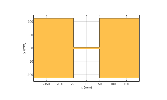
Figure contains an axes object. The axes object with xlabel x (mm), ylabel y (mm) contains 2 objects of type patch. These objects represent PEC, mypolygon.

Assign the radiator shape to pcbStack and make the changes to the board shape and feed diameter properties.

boardShape = antenna.Rectangle(Length=0.6, Width=0.3);
p = pcbStack;
p.BoardShape = boardShape;
p.Layers = {s};
p.FeedDiameter = 0.02*lambda/2;
p.FeedLocations = [0 0 1];
figure
show(p)
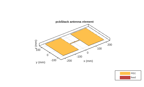
Figure contains an axes object. The axes object with title pcbStack antenna element, xlabel x (mm), ylabel y (mm) contains 3 objects of type patch, surface. These objects represent PEC, feed.

Analyze the impedance of the antenna. Effect of the end-loading should result in the series resonance to be pushed lower in the band.

figure
impedance(p,linspace(200e6,1e9,51))
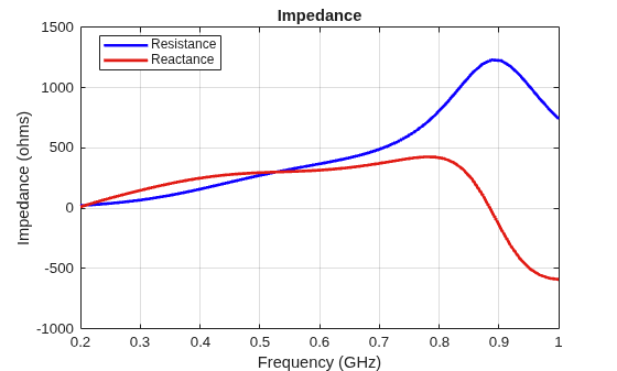
Figure contains an axes object. The axes object with title Impedance, xlabel Frequency (GHz), ylabel Impedance (ohms) contains 2 objects of type line. These objects represent Resistance, Reactance.

Create a pcb stack antenna with 2 mm dielectric thickness at the radiator and air below it. Display the structure.

p = pcbStack;
d1 = dielectric("FR4");
d1.Thickness = 2e-3;
d2 = dielectric("Air");
d2.Thickness = 8e-3;
p.Layers = {p.Layers{1},d1,d2,p.Layers{2}};
p.FeedLocations(3:4) = [1 4];
show(p)
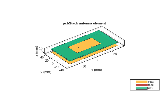
Figure contains an axes object. The axes object with title pcbStack antenna element, xlabel x (mm), ylabel y (mm) contains 9 objects of type patch, surface. These objects represent PEC, feed, FR4.

Create a PCB stack antenna from reflector backed bowtie.

b = design(bowtieRounded,1e9);
b.Tilt = 90
b = 
  bowtieRounded with properties:

        Length: 0.0959
    FlareAngle: 90
     Conductor: [1×1 metal]
          Tilt: 90
      TiltAxis: [1 0 0]
          Load: [1×1 lumpedElement]

b.TiltAxis = [0 1 0];
r = reflector(Exciter=b);
p = pcbStack(r);

Plot the directivity pattern of the antenna at 1 GHz.

pattern(p,1e9);
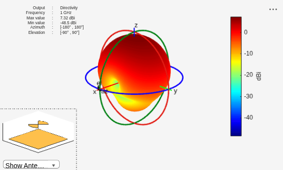
Figure contains 2 axes objects and other objects of type uilabel, uicontrol. Axes object 1 contains 5 objects of type patch, surface. Hidden axes object 2 contains 18 objects of type surface, line, text, patch.

Create a coplanar inverted F antenna.

fco = invertedFcoplanar(Height=14e-3, GroundPlaneLength=100e-3,...
                  GroundPlaneWidth=100e-3);

Use this antenna to create a pcbStack object.

p = pcbStack(fco);

Create a circular microstrip patch.

p = patchMicrostripCircular;
d = dielectric;
d.EpsilonR = 4.4;
p.Radius = 0.0256;
p.Height = 1.6e-3;
p.Substrate = d;
p.GroundPlaneLength = 3*0.0256;
p.GroundPlaneWidth = 3*0.0256;
p.FeedOffset = [0.0116 0];

Create a PCB of this patch using pcbStack.

pb = pcbStack(p);
pb.FeedDiameter = 1.27e-3;
pb.ViaLocations = [0 pb.FeedLocations(1)/1.1 1 3];
pb.ViaDiameter = pb.FeedDiameter;
figure
show(pb)
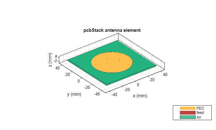
Figure contains an axes object. The axes object with title pcbStack antenna element, xlabel x (mm), ylabel y (mm) contains 12 objects of type patch, surface. These objects represent PEC, feed, Air.

Define the RF SMA connector and use it with the GerbLook writer service to generate Gerber files of the design.

C = SMA_Jack_Cinch;
O = PCBServices.GerbLookWriter;               
O.DefaultViaDiam = pb.ViaDiameter;
O.Filename = 'Microstrip circular patch-9a';
Am = PCBWriter(pb,O,C);
gerberWrite(Am)
Generated File: 'C:\Users\user\OneDrive - MathWorks\Documents\MATLAB\ExampleManager\user.Bdoc.DocWork1\antenna-ex88881296\MicrostripCircularPatch_9a.zip'
'(name is available in system cut-buffer)

13 files in PCB stack
   Size Lines File
     1k    36 MicrostripCircularPatch_9a.gtl (Copper,L1,Top,Signal)
     1k    69 MicrostripCircularPatch_9a.gbl (Copper,L2,Bot,Signal)
   107b     5 MicrostripCircularPatch_9a_1-3.txt (ExcellonPlated,1,3)
    98b     9 MicrostripCircularPatch_9a.gts (Soldermask,Top)
   227b    18 MicrostripCircularPatch_9a.gbs (Soldermask,Bot)
   103b     5 MicrostripCircularPatch_9a.txt (ExcellonPlated,1,2)
   505b    42 MicrostripCircularPatch_9a.gbp (Paste,Bot)
   130k  6817 MicrostripCircularPatch_9a.gbo (Legend,Bot)
   180k  9068 MicrostripCircularPatch_9a.gto (Legend,Top)
     1k    39 MicrostripCircularPatch_9a.gpi (PhotoplotterInfo,Info)
     1k    36 MicrostripCircularPatch_9a.dri (DrillStationInfo,Info)
     1k    22 MicrostripCircularPatch_9a.ipc (IPCD356A,Info)
              MicrostripCircularPatch_9a.gml (Profile,NP)

If you have internet connection, the Gerber files generation process opens GerbLook viewer in the web browser window. Drag and drop the Gerber files into the browser window. The viewer renders the PCB design.

This is the top view of the PCB.

Top layer

This is the bottom view of the PCB.

Bottom layer

Create a coplanar inverted-F antenna.

fco = invertedFcoplanar(Height=14e-3, GroundPlaneLength=100e-3,...
                   GroundPlaneWidth=100e-3);
show(fco)
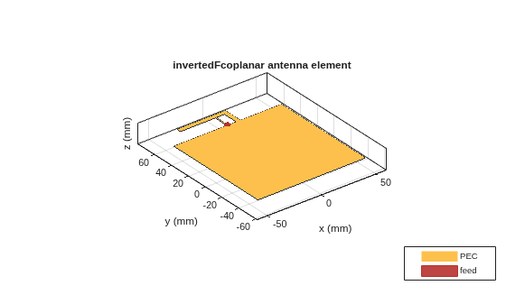
Figure contains an axes object. The axes object with title invertedFcoplanar antenna element, xlabel x (mm), ylabel y (mm) contains 3 objects of type patch, surface. These objects represent PEC, feed.

Create a linear array with inverted-F antenna as its elements.

la = linearArray;
la.Element = fco;
la.NumElements = 4;
show(la)
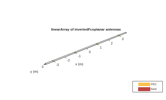
Figure contains an axes object. The axes object with title linearArray of invertedFcoplanar antennas, xlabel x (m), ylabel y (m) contains 12 objects of type patch, surface. These objects represent PEC, feed.

Use this antenna array to create the PCB antenna.

p = pcbStack(la);
show(p)
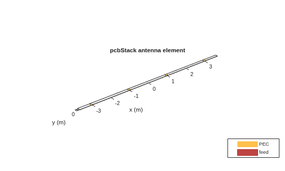
Figure contains an axes object. The axes object with title pcbStack antenna element, xlabel x (m), ylabel y (m) contains 6 objects of type patch, surface. These objects represent PEC, feed.

Create a dipole antenna object and linearArray antenna array object. In the linearArray antenna object, leave the Element property set to its default value of dipole. Set the ElementSpacing property to 4."

d1 = dipole;
d2 = linearArray(ElementSpacing=4);

To set the Z-coordinate of pcbStack antenna object to zero, rotate the dipole and linear dipole array around 90 degrees using the Tilt property. Then set the TiltAxis property to [ 0 -1 0 ] for dipole and linear dipole array antennas.

d1.Tilt = 90;
d2.Element.Tilt = 90;
d1.TiltAxis = [0 -1 0];
d2.Element.TiltAxis = [0 -1 0];

Create and view PCB stack antenna created using the dipole antenna object.

p1 = pcbStack(d1);
show(p1)
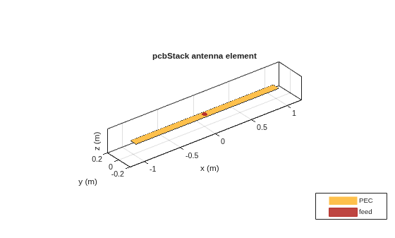
Figure contains an axes object. The axes object with title pcbStack antenna element, xlabel x (m), ylabel y (m) contains 3 objects of type patch, surface. These objects represent PEC, feed.

Create and view PCB stack antenna using the linearArray antenna array object.

p2 = pcbStack(d2);
show(p2)
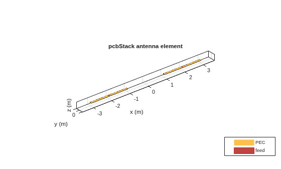
Figure contains an axes object. The axes object with title pcbStack antenna element, xlabel x (m), ylabel y (m) contains 4 objects of type patch, surface. These objects represent PEC, feed.

Create a circular microstrip patch antenna.

ant = design(patchMicrostripCircular,3e9);
ant.Substrate = dielectric("FR4");
show(ant)
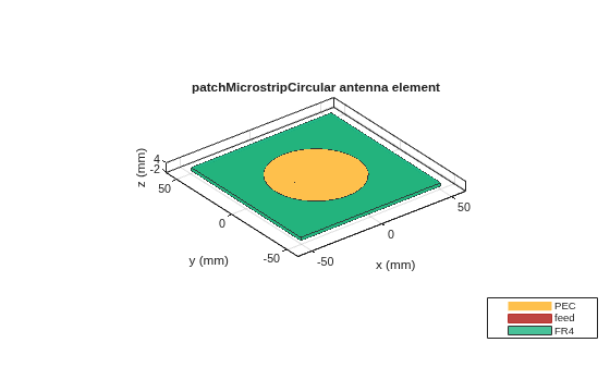
Figure contains an axes object. The axes object with title patchMicrostripCircular antenna element, xlabel x (mm), ylabel y (mm) contains 6 objects of type patch, surface. These objects represent PEC, feed, FR4.

c = antenna.Circle;
show(c)

Figure contains an axes object. The axes object with xlabel x (m), ylabel y (m) contains 2 objects of type patch. These objects represent PEC, mycircle.

c.NumPoints = 6;
c.Radius = 3*ant.Radius;
figure
show(c)
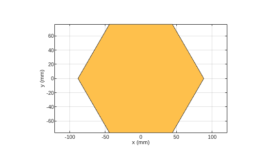
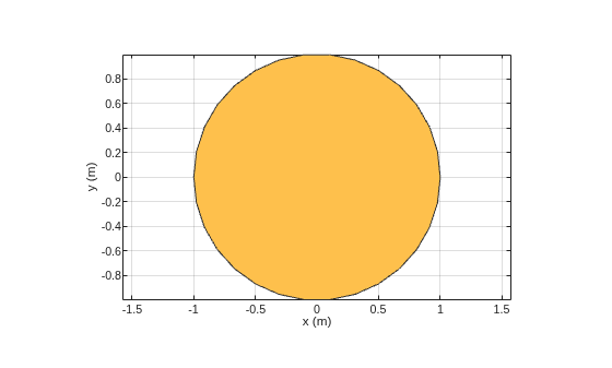
Figure contains an axes object. The axes object with xlabel x (mm), ylabel y (mm) contains 2 objects of type patch. These objects represent PEC, mycircle.

Create the PCB stack using the vertices derived from the circle shape.

v = getShapeVertices(c);
cp = antenna.Polygon(Vertices=v);
pb = pcbStack(ant);
pb.Layers{3} = cp;
pb.BoardShape = cp;
show(pb)
axis equal
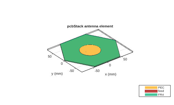
Figure contains an axes object. The axes object with title pcbStack antenna element, xlabel x (mm), ylabel y (mm) contains 9 objects of type patch, surface. These objects represent PEC, feed, FR4.

Define dimensions of the circular patch antenna, RF connector, and FR4 dielectric substrate.

% Operating frequency
f = 2.44e9;

% Geometry
gnd = 80e-3;
h = 1.53e-3;
r = 16.8e-3;
feedloc = [5.1e-3 0];

% RF Connector dimensions
DinFeed = 1.25e-3;
DoutFeed = 4.1e-3;

% FR4 substrate
d = dielectric(Name='FR4',EpsilonR=4.3,LossTangent=0.015,Thickness=h);

Create a circular patch antenna based on these parameters.

patch = patchMicrostripCircular(GroundPlaneLength=gnd,GroundPlaneWidth=gnd,...
    Radius=r,Height=h,Substrate=d,FeedOffset=feedloc);

Convert the circular patch antenna into a PCB stack and define the feed parameters.

p = pcbStack(patch);
p.FeedViaModel = 'square';
p.FeedDiameter = DinFeed;

Refine the mesh of this antenna. Define an RF connector for this PCB stack. Compute and plot radiation pattern using the FEM solver.

[~] = mesh(p,MaxEdgeLength=0.0035);
p.SolverType = 'FEM';
connector = RFConnector(InnerRadius=0.5*DinFeed,OuterRadius=0.5*DoutFeed,...
    EpsilonR=2,PinLength=0);
p.Connector = connector;
pattern(p,f)
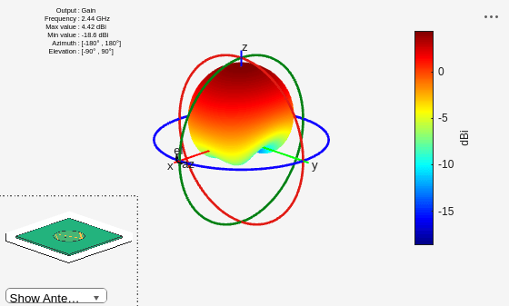
Figure contains 2 axes objects and other objects of type uicontrol. Axes object 1 contains 10 objects of type patch, surface. This object represents FR4. Hidden axes object 2 contains 20 objects of type surface, line, text, patch. This object represents FR4.

Create a rectangular patch antenna on an FR4 dielectric substrate using a pcbStack object.

patch = antenna.Rectangle(Length=0.02,Width=0.02);
gnd = antenna.Rectangle(Length=0.04,Width=0.04);
d = dielectric("FR4");
d.Thickness = 1.6e-3;

p = pcbStack;
p.BoardShape = gnd;
p.BoardThickness = 1.6e-3;
p.Layers = {patch,d,gnd};
p.FeedViaModel = "strip";

Create a ProbeFeed object and assign it to the FeedDefinitions property.

pf = ProbeFeed;
pf.ViaModel = "octagon";
pf.SignalLocations = [0 0];
pf.SignalLayers = 1;
pf.GroundLayers = 3;

p.FeedFormat = "FeedDefinitions";
p.FeedDefinitions = pf;

Visualize the antenna geometry and feed.

figure
show(p)
title("PCB Antenna with Probe Feed")
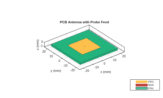
Figure contains an axes object. The axes object with title PCB Antenna with Probe Feed, xlabel x (mm), ylabel y (mm) contains 8 objects of type patch, surface. These objects represent PEC, feed, FR4.

Supported Catalog Elements

The following antennas and arrays from the catalog can be converted into a PCB antenna by the pcbStack object:

Antennas

Note

Orient these antennas in the xy-plane if required, before conversion to pcbStack.

  • Dipole Antennas: dipole, bowtieTriangular, bowtieRounded, and dipoleBlade.

  • Fractal Antennas: fractalCarpet, fractalGasket, fractalIsland, fractalKoch, and fractalSnowflake

  • Loop Antennas: loopCircular, loopRectangular

  • Monopole Antennas: invertedFcoplanar, invertedLcoplanar

  • Patch Antennas: patchMicrostrip, patchMicrostripCircular, patchMicrostripElliptical, patchMicrostripEnotch, patchMicrostripHnotch, patchMicrostripInsetfed, patchMicrostripTriangular

  • Reflector Antennas: reflector and reflectorCircular with a finite ground plane.

  • Slot Antennas: slot, vivaldi, vivaldiAntipodal, vivaldiOffsetCavity

  • Spiral Antennas: spiralArchimedean, spiralEquiangular, spiralRectangular

  • Other Antennas: lpda, customAntennaGeometry, customArrayGeometry

Arrays

Note

The arrays must be homogeneous, with uniform elements.

  • linearArray

  • circularArray

  • rectangularArray

References

[1] Balanis, C. A. Antenna Theory. Analysis and Design. 3rd Ed. Hoboken, NJ: John Wiley & Sons, 2005.

[2] Stutzman, W. L. and Gary A. Thiele. Antenna Theory and Design. 3rd Ed. River Street, NJ: John Wiley & Sons, 2013.

Version History

Introduced in R2017a

expand all