dsp.Channelizer
Polyphase FFT analysis filter bank
Description
The dsp.Channelizer
System object™ separates a broadband input signal into multiple narrow subbands using a fast
Fourier transform (FFT)-based analysis filter bank. The filter bank uses a prototype lowpass
filter and is implemented using a polyphase structure. You can specify the filter coefficients
directly or through design parameters.
To separate a broadband signal into multiple narrow subbands:
Create the
dsp.Channelizerobject and set its properties.Call the object with arguments, as if it were a function.
To learn more about how System objects work, see What Are System Objects?
Creation
Syntax
Description
channelizer = dsp.Channelizerdsp.ChannelSynthesizer
System object.
channelizer = dsp.Channelizer(M)NumFrequencyBands property set to M.
Example: channelizer = dsp.Channelizer(16)
channelizer = dsp.Channelizer(M,D)DecimationFactor property set to D.
Example: channelizer = dsp.Channelizer(16,8)
channelizer = dsp.Channelizer(PropertyName=Value)DecimationFactor to 4.
Properties
Usage
Description
Input Arguments
Output Arguments
Object Functions
To use an object function, specify the
System object as the first input argument. For
example, to release system resources of a System object named obj, use
this syntax:
release(obj)
Examples
Channelize and synthesize a sine wave signal with multiple frequencies using an M -channel filter bank.
The M -channel filter bank contains an analysis filter bank section and a synthesis filter bank section. The dsp.Channelizer object implements the analysis filter bank section. The dsp.ChannelSynthesizer object implements the synthesis filter bank section. These objects use an efficient polyphase structure to implement the filter bank. For more details, see Polyphase Implementation under Algorithms on the object reference pages.
Initialization
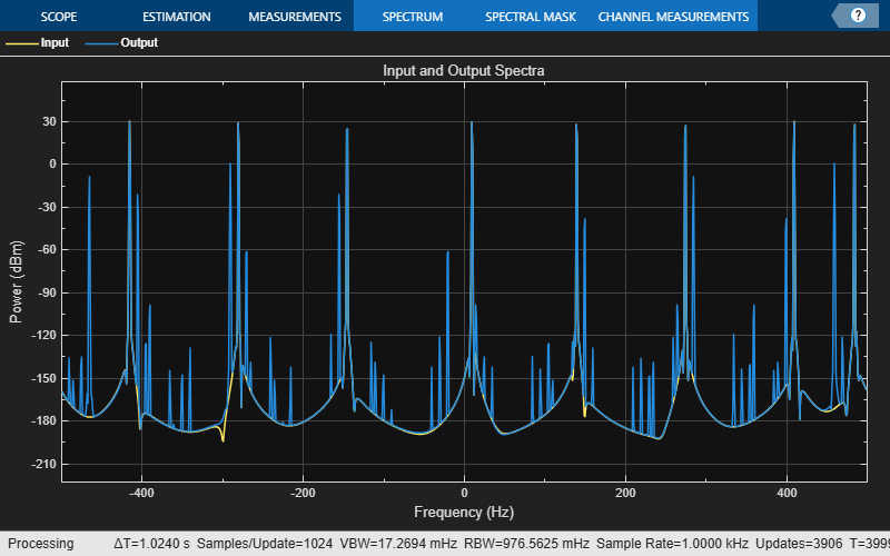
Initialize the dsp.Channelizer and dsp.ChannelSynthesizer System objects. Each object is set up with 8 frequency bands, 8 polyphase branches in each filter, 12 coefficients per polyphase branch, and a stopband attenuation of 140 dB. Use a sine wave with multiple frequencies as the input signal. View the input spectrum and the output spectrum using a spectrum analyzer.
offsets = [-40,-30,-20,10,15,25,35,-15];
sinewave = dsp.SineWave(ComplexOutput=true,Frequency=offsets+(-375:125:500),...
    SamplesPerFrame=800);

channelizer = dsp.Channelizer(StopbandAttenuation=140);
synthesizer = dsp.ChannelSynthesizer(StopbandAttenuation=140);
scope = spectrumAnalyzer(ShowLegend=true,...
    SampleRate=sinewave.SampleRate,...
    ChannelNames=["Input","Output"],...
    Title="Input and Output Spectra");
Streaming
Use the channelizer to split the broadband input signal into multiple narrow bands. Then pass the multiple narrowband signals into the synthesizer, which merges these signals to form the broadband signal. Compare the spectra of the input and output signals. The input and output spectra match very closely.
for i = 1:5000
    x = sum(sinewave(),2);
    y = channelizer(x);
    v = synthesizer(y);
    scope(x,v)
end
Create a dsp.Channelizer object and set the LowpassCoefficients property to a vector of complex coefficients.
Complex Coefficients
Using firpm, determine the coefficients of a Park-McClellan's optimal equiripple FIR filter of order 30, and frequency and amplitude characteristics described by F = [0 0.2 0.4 1.0] and A = [1 1 0 0] vectors, respectively.
Create a complex version of these coefficients by multiplying with a complex exponential. The resultant frequency response is that of a bandpass filter at the specified frequency, in this case 0.4.
blowpass = firpm(30,[0 .2 .4 1],[1 1 0 0]);
N = length(blowpass)-1;
Fc = 0.4;
j = complex(0,1);
bbandpass = blowpass.*exp(j*Fc*pi*(0:N));
Channelizer
Create a dsp.Channelizer object with 4 frequency bands and set the Specification property to 'Coefficients'.
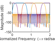
chann = dsp.Channelizer(4,Specification="Coefficients");Pass the complex coefficients to the channelizer. The prototype filter is a bandpass filter with a center frequency of 0.4. The modulated versions of this filter appear with respect to the prototype filter and are wrapped around the frequency range [Fs Fs].
chann.LowpassCoefficients = bbandpass
chann =
  dsp.Channelizer with properties:

   Main
      NumFrequencyBands: 4
       DecimationFactor: 'Number of frequency bands'
          Specification: 'Coefficients'
    LowpassCoefficients: [0.0019 + 0.0000i 0.0005 + 0.0016i 0.0011 - 0.0008i 0.0051 + 0.0037i -0.0024 + 0.0073i -3.4175e-04 + 8.3704e-20i 0.0042 + 0.0128i -0.0174 + 0.0126i -0.0077 - 0.0056i -0.0070 + 0.0214i -0.0514 + 0.0000i … ] (1×31 double)

  Show all properties
Visualize the frequency response of the channelizer.
freqz(chann)
More About
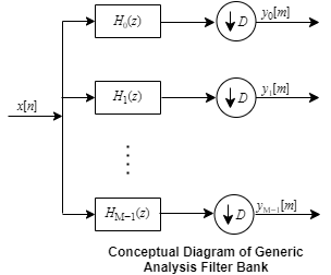
The generic analysis filter bank consists of a series of parallel bandpass filters that split an input broadband signal, x[n], into a series of narrow subbands. Each bandpass filter retains a different portion of the input signal. After the bandwidth is reduced by one of the bandpass filters, the signal is downsampled to a lower sampling rate commensurate with the new bandwidth.
The transfer function of the modulated kth bandpass filter is given by:
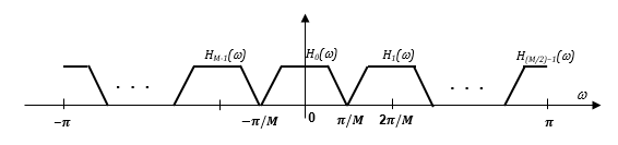
This figure shows the frequency response of M filters.

To obtain the frequency response characteristics of the filter Hk(z), where k = 1, … , M−1, uniformly shift the frequency response of the prototype filter, H0(z), by multiples of 2π/M. Each subband filter, Hk(z), {k = 1, … , M – 1}, is derived from the prototype filter.
Following is an equivalent representation of the frequency response diagram with ω ranging from [−π π].
The frequency components in the input signal, x[n], are translated in frequency to baseband by multiplying x[n] with the complex exponentials, , where , and . The resulting product signals are passed through the lowpass filters, H0(z). The output of the lowpass filter is relatively narrow in bandwidth. Downsample the signal commensurate with the new bandwidth. Choose a decimation factor, D ≤ M, where M is the number of branches of the analysis filter bank. When D < M, the channelizer is known as oversampled or non-maximally decimated channelizer.
The figure shows an analysis filter bank that uses the prototype lowpass filter.

y1[m], y2[m], … , yM−1[m] are narrow subband signals translated into baseband.
Algorithms
When D = M, the channelizer is known as the maximally decimated channelizer or critically sampled channelizer.
Here is the multirate noble identity for decimation, assuming that D = M.
![]()
For example, consider the first branch of the filter bank that contains the lowpass filter.
![]()
Replace H0(z) with its polyphase representation.
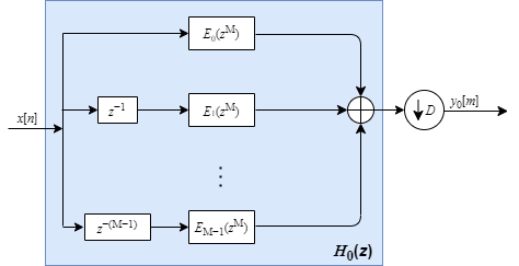
After applying the noble identity for decimation, you can replace the delays and the decimation factor with a commutator switch. The switch starts on the first branch 0 and moves in the counterclockwise direction as shown in the following diagram. The accumulator at the output receives the processed input samples from each branch of the polyphase structure and accumulates these processed samples until the switch goes to branch 0. When the switch goes to branch 0, the accumulator outputs the accumulated value.

For all M channels in the filter bank, the transfer function H(z) is given by:
The matrix on the left is an inverse discrete Fourier transform (IDFT) matrix. With the IDFT matrix, the efficient implementation of the lowpass prototype-based filter bank looks like the following.
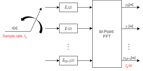
When the channelizer receives the first input sample, the switch feeds this input to the branch 0 and the channelizer computes the first set of output values. As more input samples come in, the switch moves in the counterclockwise direction through branches M−1, M−2, all the way up to branch 0, delivering one sample at a time to each branch. When the switch comes to branch 0, the channelizer outputs the next set of output values. This process continues as the data keeps coming in. Every time the switch comes to the first branch 0, the channelizer outputs y0[m], y1[m], … , yM-1[m]. Each branch in the channelizer effectively outputs one sample for every M samples it receives. Hence, the sample rate at the output of the channelizer is fs/M.
If you use the M-point FFT, the implementation looks like the following.
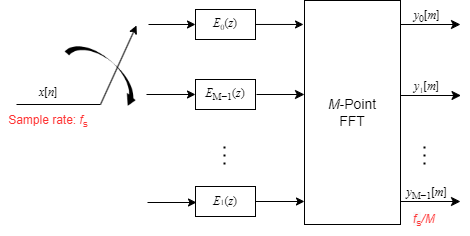
When the switch delivers the first sample to branch 0, the channelizer computes the first set of output values. As more data comes in, the switch moves in the clockwise direction to branches M−1, M−2, all the way up to branch 1, delivering one sample at a time to each branch. When the switch comes to branch 0, the channelizer outputs the next set of output values. This process continues as more data keeps coming in.
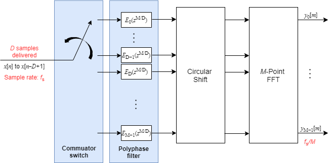
When D < M, the channelizer is known as the non-maximally decimated channelizer or oversampled channelizer. In this configuration, the output sample rate is different from the channel spacing. The non-maximally decimated channelizers offer increased design freedom, but at the expense of increasing computational cost.
If the ratio M/D equals an integer that is greater than 1 and is less than or equal to M−1, the channelizer is known as integer-oversampled channelizer. If the ratio M/D is not an integer, then the channelizer is known as rationally-oversampled channelizer.
In this configuration, when the first input sample is delivered, the switch feeds this input to branch 0 and the channelizer computes the first set of output values. As more input samples come in, the switch moves in the counterclockwise direction through branches D−1, D−2, all the way up to branch 0, delivering one sample at a time to each branch. When the switch comes to branch 0, the channelizer outputs the next set of output values. This process continues as the data keeps coming in. Every time the switch comes to the first branch 0, the channelizer outputs y0[m], y1[m], … , yM-1[m].
As more data keeps coming in and the switch feeds these samples to the first D addresses, the formal contents of these addresses are shifted to the next set of D addresses, and this process of data shift continues every time there is a new set of D input samples.
For every D input samples that are fed to the polyphase structure, the channelizer outputs M samples, y0[m], y1[m], … , yM-1[m]. This process increases the output sample rate from fs/M in the case of a maximally decimated channelizer, to fs/D in the case of a non-maximally decimated channelizer.
For more details, see [2].
After each D-point data sequence is delivered to the partitioned M-stage polyphase filter, the outputs of the M stages are computed and conditioned for delivery to the M-point FFT. The data shifting through the filter introduces frequency-dependent phase shift. To correct for this phase shift and alias all bands to DC, a circular shift buffer is inserted after the polyphase filters and before the M-point FFT.
With the commutator switch followed by M-stage polyphase filter, circular shift buffer, and a DFT matrix, the efficient implementation of the lowpass prototype-based filter bank looks like this.
References
[1] Harris, Fredric J, Multirate Signal Processing for Communication Systems, Prentice Hall PTR, 2004.
[2] Harris, F.J., Chris Dick, and Michael Rice. "Digital Receivers and Transmitters Using Polyphase Filter Banks for Wireless Communications." IEEE® Transactions on Microwave Theory and Techniques. 51, no. 4 (2003).
Extended Capabilities
Version History
Introduced in R2016bSee Also
Functions
coeffs|tf|polyphase|freqz|bandedgeFrequencies|centerFrequencies|getFilters
Objects
dsp.ChannelSynthesizer|dsp.FIRHalfbandDecimator|dsp.FIRHalfbandInterpolator|dsp.IIRHalfbandDecimator|dsp.DyadicAnalysisFilterBank
Blocks
- Channelizer | Channel Synthesizer | Dyadic Analysis Filter Bank | Two-Channel Analysis Subband Filter