Designing a Novel ADC Architecture with Feedback and Noise Shaping
By Rahmi Hezar, Texas Instruments
In a mobile phone, the analog-to-digital converter (ADC) converts an analog baseband signal to digital baseband. Because component size and power drain are important for phones, a single ADC might need to cover multiple frequencies and wireless standards (for example, GSM and Bluetooth). The ADC must consume as little power and chip area as possible and use as few components as possible. It must also be resistant to noise, nonlinearities, and manufacturing tolerances. These requirements combine to create difficult design challenges. We designed an ADC that meets these requirements by using noise shaping to reduce chip area and power consumption.
Speed of simulation is key to the success of a project involving a completely new design. To determine the impact of real-world effects and manufacturing tolerance on our design, we needed to run multiple parameter sweeps. To complete these in a reasonable time frame, we needed rapid system simulation, which is why we used system-level design with MATLAB® and Simulink®.
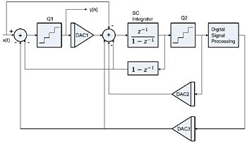
As a mixed-signal device, an ADC is vulnerable to circuit imperfections like noise, nonlinearity, and coupling mismatches. Because sigma-delta architectures are considered very robust against these imperfections, they are widely used in ADCs. The sigma-delta modulator shapes quantization noise and pushes it outside the bandwidth of interest, where it is removed by FIR filtering. The order of the sigma-delta determines the noise-shaping properties: the higher the order, the better the noise shaping. However, after the second order, these circuits become unstable and can go into oscillation under certain conditions. In practice, we use second-order sigma-delta modulators to get a stable system (Figure 1). Most second-order systems have two integrators in the circuit, each with its own amplifier. The amplifiers consume a lot of power and chip space. Our goal was to redesign the sigma-delta circuit so that it used just one integrator and one amplifier.

The ADC Architecture
We devised an architecture based on error feedback and noise shaping. Error feedback architectures have been used in digital-to-analog conversion (DAC) and noise shaping for some time, but combining them into one circuit is novel.
We inserted DACs where necessary into this feedback architecture, and converted the architecture to an ADC structure (Figure 2). We inserted a first-order sigma-delta modulator in the loop that will requantize the noise introduced by the first quantizer. Once this quantization noise has been digitized, we can operate on it using noise-shaping DSP functions. Because so much of the processing now takes place digitally, this design can be tuned for different frequencies and bandwidths by changing the digital filter coefficients. The design has just one integrator, and therefore just one amplifier.

Investigating Noise, Manufacturing Tolerances, and Impairments
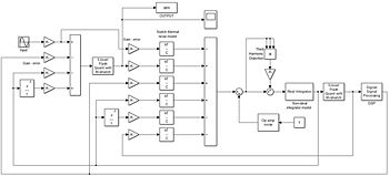
Although my team works primarily at the architectural level, our role includes making certain that designs work in the real world, which means that we have to simulate the effects of manufacturing tolerances, noise, and nonidealities. This circuit was to be manufactured using a 65 nm CMOS process optimized for digital circuits, which meant we had to simulate circuit imperfections introduced by the manufacturing process. For example, we wanted our quantizer to quantize uniformly, but we knew that, in practice, there would be some deviation from this ideal. Similarly, the DACs would have manufacturing imperfections that might affect overall system performance. We modeled noise and nonidealities such as thermal noise, 1/f noise, coupling effects, slew rate, and amplifier gain bandwidth limitations. Our system-level simulation work included all these impairments (Figure 3).

To investigate the interaction of all these factors, we ran Monte Carlo simulations in Simulink using parameter sweeps. We characterized the circuit with a series of Gaussian curves showing how different input parameters affected performance. We could then see how sensitive our design was to different factors and how much variation the design could withstand while remaining within our specification. For example, it might be able to withstand a 5% variation in one component but only a 1% or 2% variation in another. The magnitude of some circuit values was an issue, too. For example, a large capacitor in one of the DACs would be less affected by variations than a smaller capacitor. In addition to the technical requirements, we had manufacturing yield goals that related to profitability—for a given price point, we knew we would have to attain a certain manufacturing yield, which meant that our circuit model had to be resistant to certain levels of manufacturing tolerance.
We had to consider how these variations affected noise shaping. For example, a circuit mismatch might lead to an unwanted third-order harmonic, which would lead to our noise shaping circuit placing noise within our signal spectrum.
Monte Carlo simulations are computationally expensive and time-consuming, but they are absolutely essential to determining whether a design is feasible. The need to run these studies determined our choice of design tools. SPICE simulations are accurate but take a long time to run, making parameter sweep–based simulations prohibitively time-consuming. Simulink runs much faster than SPICE, meaning we can get answers back very quickly and iterate our design. With SPICE, we would have to choose the first design that worked. With Simulink, we can choose the best design.
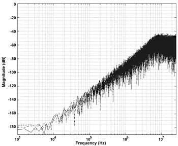
Our final Simulink design gave us the performance we wanted and was robust to manufacturing tolerances. The quantization noise as output by our model is shaped as we wanted (Figure 4).

Using the Simulink Model as an Executable Specification
Our Simulink model acted as an executable specification for the next stage of our design for both analog and digital designers. The analog designers used the Simulink model to guide their SPICE development. The model clearly and unambiguously showed the behavior we wanted to achieve. The designers used it to gauge the effect of different analog circuit choices on overall system performance. For example, if their design had a certain mismatch, they ran the Simulink model with this mismatch to check that the system as a whole stayed within its specification.
From the beginning, we were careful to build our Simulink model so that it would translate easily to VHDL® code. For example, we built the FIR filters in Simulink using only delay elements, gain coefficients, and adders. Our Simulink model mapped cleanly to a fixed-point RTL representation: Our digital designer was able to look at the Simulink model and quickly write the VHDL code to match. The goal, of course, was to reduce the scope for errors. We verified our design by comparing the outputs of the VHDL code and the Simulink model, and checking whether the VHDL code was bit-accurate to the Simulink model.
Results and Next Steps
To verify our design, we produced a number of test chips. Lab results agreed with our simulations, showing that our ADC design actually worked. Because of the novel nature of our design, we applied for and were granted a patent on the technology.
Because our system-level design approach rapidly gave us results for this project, we used the same design methodology on subsequent projects.
Published 2013 - 92102v00