Memory and Register Channel Connections
The memory channel models the data transfer from FPGA to processor using shared external memory. The register channel models the control of FPGA logic from processor. You can both configure the FPGA logic and read the status of FPGA logic from processor. The following sections show how to create these channel connections.
Memory Channel Connection
Open the
soc_hwsw_top.slxmodel.Add a Memory Channel block and a Memory Controller block to the
Memoryarea. Together, these blocks model the memory connection throughDDRbetween the processor and FPGA sides of your application.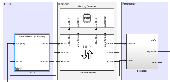
Open the Memory Controller block dialog mask. Set Number of masters to
2. In the Advanced tab, the Memory Controller automatically inherits parameters from the Hardware board specified in the model configurations.Connect the pair of Memory Controller burst ports,
burstReqandburstDone, to the read and write burst request ports of the Memory Channel block.In the model, open the Memory Channel block dialog mask. Set Channel type to
AXI4-Stream to Software via DMA. Set Buffersize (bytes) toFrameSize*4and Number of buffers to6. Click OK.
Register Channel Connection
Add a Register Channel block to the model and connect the block to the
ProcessorandFPGAsubsystems as shown in the following image.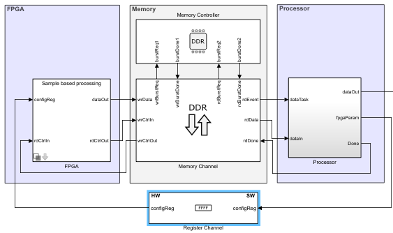
Open the Register Channel block dialog mask. Add a new register with these properties.
Register Direction Data type Dimension configReg Write uint8 1 Set Register write sample time to
FPGASSTime. Click OK. This sample time is set in the filesoc_hwsw_init.m.