ADC Data Capture to DDR Memory on RFSoC Device
This example shows how to perform analog-to-digital converter (ADC) data captures with programmable logic (PL) double data rate 4 (DDR4) memory.
Storing data into PL-DDR4 memory can be advantageous because of the large amount of space available to read and write to. A total of 4 gigabytes is available to access from the FPGA. The HDL Coder™ reference designs provide a means for your IP design to connect to this memory interface by using AXI4-Master. AXI4-Master requires state-machine logic to perform reading and writing using multiple control signal lines.

State-machine logic in the IP design helps coordinate this transfer by issuing commands originating from MATLAB® as AXI4 register writes. These register writes command the state machine to be configured in different modes. For this data capture example, these modes are broken down into two main operations.
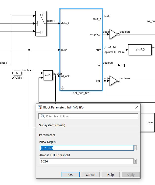
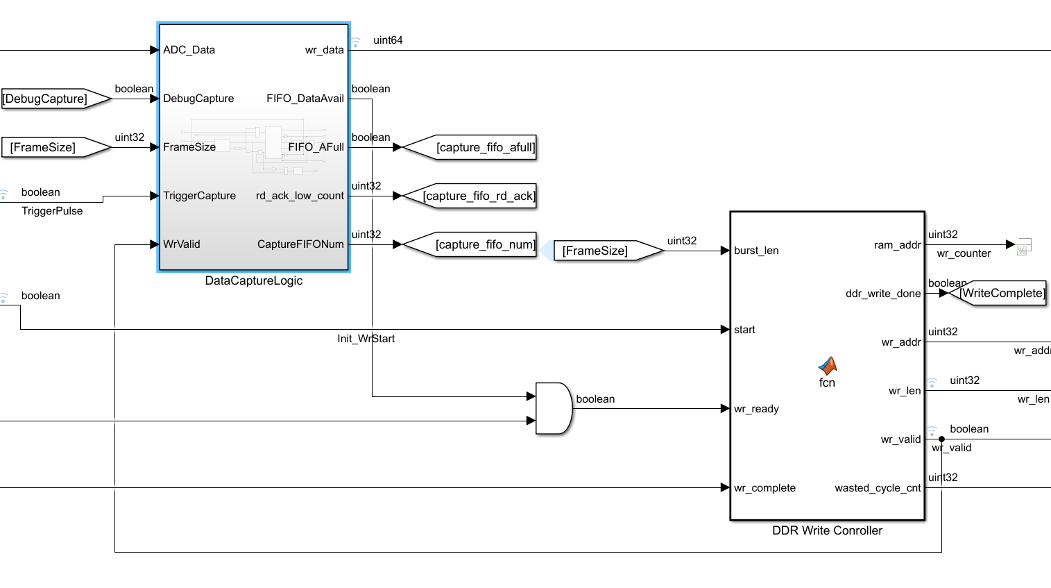
The first arrow (labeled 1) in the first figure shows a data path connecting the ADC input stream directly into AXI4-Master to write to the memory interface generator (MIG). From MATLAB, an AXI4 register is written to the state machine to issue a command that data is ready to be written. The state machine then waits for acknowledgement from the DDR4 slave device that it is ready to accept samples. Afterward, data can flow through to the MIG. Because there is a bit of wait time on issuing burst write commands, a back pressure first in, first out (FIFO) is used to help temporarily store data during these periods. In some cases, the amount of back pressure experienced can exceed the FIFO, causing data to be lost. This example inserts several registers to help determine if this situation arises. Typically, this issue happens if the requested data capture size is large enough to induce enough back pressure events to exceed the FIFO capacity. Constant writing to DDR4 memory can be sustained to only a certain frame length before back pressure occurs. Increasing the length of the FIFO can help alleviate this issue at the cost of more FPGA resources. This figure shows the section of the model that is responsible for writing to the digital-to-analog converter (DAC).
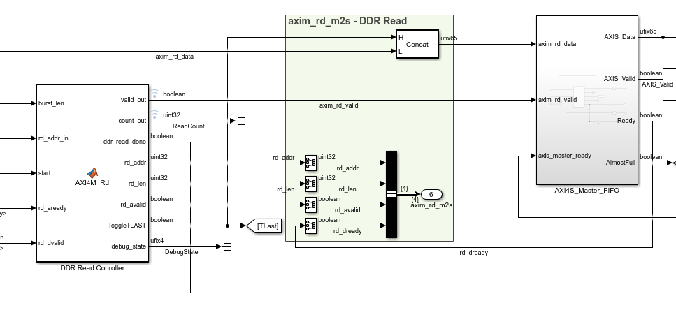
The second arrow (labeled 2) in the first figure shows the data path of reading from DDR4 memory and returning the frame back to MATLAB or Simulink® over the Ethernet network. Similar to the data path labeled 1, the data path labeled 2 is also controlled with a state machine that is adjustable with AXI4 registers. For each read command issued, an offset address is used to specify which spot in PL-DDR4 memory to read from. This figure shows the read controller logic.
Requirements
Vivado® Design Suite with a supported version listed in Supported EDA Tools and Hardware
Xilinx® Zynq® UltraScale+™ RFSoC ZCU111, ZCU208, ZCU216, or DFE ZCU670 evaluation kit
Open Example
Open the example project and copy the example files to a temporary folder.
1. Navigate to the example source folder by entering these commands at the MATLAB command prompt.
example_root = (hdlcoder_rfsoc_examples_root)
cd (example_root)
2. Copy all of the example files in the DDR4_ADCCapture folder to a temporary folder.
Simulate PL-DDR4 ADC Capture Model
To examine how these operations take place, open the model rfsocADCDDR4Capture.slx and simulate the design.
By default, the simulation uses the debugCaptureSimMode set to 1. With this mode, the capture logic captures counter data instead of ADC data. The goal is to validate that the counter data written to PL-DDR4 memory is the same data read out when issuing a read command later.

The other input AXI4 registers specify the amount of data to capture (ADC_CaptureSize), the amount of data to write back to the DMA AXI4-Stream per read (DDR4_Rd_FrameLen), and the offset address of where to read from in PL-DDR4 memory (DDR4_ReadAddress).
The model stops simulating at the end of the last sample of the frame of data that is sent over the DMA. Afterward, validate that the data written into PL-DDR4 memory is the same as the data that was read out by running the MATLAB script simValidateADCDDR4Capture.m.

The counter value matches expectations when read out of the DDR4 memory and accessed via the AXI4-Stream DMA. Next, disable debug mode and configure the simulation to capture ADC data instead. Open the script rfsocADCDDR4CaptureInit.m, and then set debugCaptureSimMode to false. Rerun the simulation, and then plot the data by running the script simValidateADCDDR4Capture.m.

Generate HDL and Synthesize Bitstream
Open the model rfsocADCDDR4Capture.slx, and then right-click the ADC_DDR4_Data_Capture subsystem. Select HDL Code, then click HDL Workflow Advisor.
In step 1.1 of the HDL Workflow Advisor, select Target platform as Xilinx Zynq Ultrascale+ RFSoC ZCU111 Evaluation Kit, Xilinx Zynq Ultrascale+ RFSoC ZCU208 Evaluation Kit, Xilinx Zynq UltraScale+ RFSoC ZCU216 Evaluation Kit, or Xilinx Zynq UltraScale+ RFSoC DFE ZCU670 Evaluation Kit.
In step 1.2, select Reference design as Real ADC/DAC Interface.
Before proceeding to the next step, set these reference design parameters to the indicated values.
AXI4-Stream Master data width to
64AXI4-Stream Slave data width to
64Add external memory access (AXI4 Master) to
trueADC sampling rate (MHz) to
2048ADC decimation mode (xN) to
4ADC samples per clock cycle to
4ADC mixer type to
BypassedDAC sampling rate (MHz) to
2048DAC interpolation mode (xN) to
4DAC samples per clock cycle to
4DAC mixer type to
BypassedADC/DAC NCO mixer LO (GHz) to
DisabledEnable multi-tile sync to
false
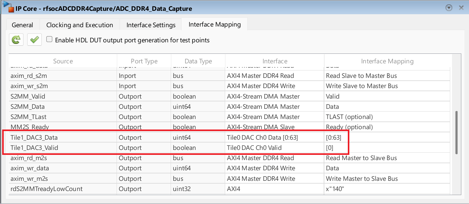
If you are using a ZCU208, ZCU216, or ZCU670 board, additionally set the DAC DUC mode parameter to Full DUC Nyquist (0-Fs/2).
If you are using a ZCU208 board, for the port Tile1_DAC3_Data, set the target interface to Tile0 DAC Ch0 Data. For the port Tile1_DAC3_Valid, set the target interface to Tile0 DAC Ch0 Valid.
In step 4.2, to generate a script that provides MATLAB connectivity to the board for interactive testing and live I/O interfacing, select Generate host interface script and clear the Generate Simulink software interface model checkbox.
Initiate the bitstream compilation. After the compilation is complete, use a programming script to program the FPGA bit file.
Collect Captured PL-DDR4 ADC Data
After you create and program the FPGA bit file onto the board, you can capture data.
In this capture scenario, the goal is to capture 4 million data points of ADC samples. Because the design is operating at four samples per clock, the data width of each data point written to DDR4 memory is 64 bits. Each data point has an 8 byte offset. To retrieve the samples, use the shared-memory FPGA I/O API over a TCP/IP connection.
The script performs these steps.
Initiate a data capture and store 4 million samples into DDR4 memory.
Check to see if samples were dropped in the data collection due to back pressure.
Use shared memory to directly read samples from DDR4 memory from ARM®-Linux® and transfer samples back to MATLAB.
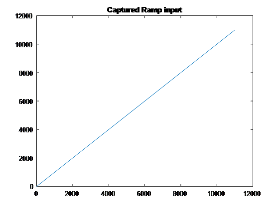
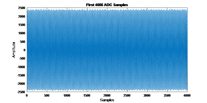
This plot shows the first 4000 samples when the capture loop execution finishes.
In this example, a capture size of 4 million is possible. Increasing the capture size can yield results where data is missing. For instance, setting the capture length to 8 million (by changing the frame size to 2e6 rather than 1e6).
% %% Parameters
% DebugMode = 0;
% incrScale = 2^14/512e6; % Used to adjust NCO frequency
% Fs = 512e6;
% CaptureSize = 2e6;      % Total amount of four-vector contigious samples to store in PL-DDR4
% DDR4_ReadLen = 100e3;   % Amount of four-vector samples to retrieve per read from PL-DDR4
Run this script again.
HostIOs_rfsocADCDDR4Capture_interface
From these 8 million samples captured, 6329 four-vector samples were dropped, (that is, 25,316 ADC samples are missing). In plots of the captures, a missing sample is displayed as a discontinuity, which you can view by using the zoom feature of the plots.
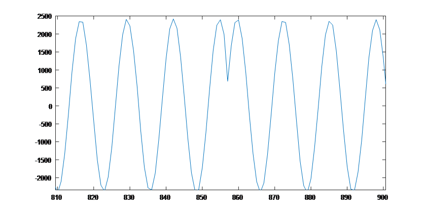
The spectrum might not look as severely affected because many samples exist in the frame, but this many samples can still cause issues depending on your end applications. Choosing a back-pressure FIFO depth that is optimal to your design specifications is one workaround to help mitigate missing samples. For more details on where to change this FIFO depth, see this part of the model: rfsocADCDDR4Capture/ADC_DDR4_Data_Capture/DDR_Capture_Logic/DataCaptureLogic.