P-Channel LDMOS FET
P-Channel laterally-diffused metal-oxide-semiconductor or vertically-diffused metal-oxide-semiconductor transistors suitable for high voltage
Libraries:
Simscape /
Electrical /
Semiconductors & Converters
Description
The P-Channel LDMOS FET block models LDMOS (or VDMOS) transistors suitable for high voltage. The model is based on surface potential and includes effects due to an extended drain (drift) region:
Nonlinear capacitive effects associated with the drift region
Surface scattering and velocity saturation in the drift region
Velocity saturation and channel-length modulation in the channel region
Charge conservation inside the model, so you can use the model for charge sensitive simulations
The intrinsic body diode
Reverse recovery in the body diode model
Temperature scaling of physical parameters
For the option with exposed thermal port (see Thermal Port), dynamic self-heating
For information on physical background and defining equations, see the N-Channel LDMOS FET block reference page. Both the p-type and n-type versions of the LDMOS model use the same underlying code with appropriate voltage transformations, to account for the different device types.
The charge model is similar to that of the surface-potential-based MOSFET model, with additional expressions to account for the charge in the drift region. The block uses the derived equations as described in [1], which include both inversion and accumulation in the drift region.
Modeling Body Diode
The block models the body diode as an ideal, exponential diode with both junction and diffusion capacitances:
where:
Idio is the current through the diode.
Is is the reverse saturation current.
VBD is the body-drain voltage.
n is the ideality factor.
ϕT is the thermal voltage.
Cj is the junction capacitance of the diode.
Cj0 is the zero-bias junction capacitance.
Vbi is the built-in voltage.
Cdiff is the diffusion capacitance of the diode.
τ is the transit time.
The capacitances are defined through an explicit calculation of charges, which are then differentiated to give the capacitive expressions above. The block computes the capacitive diode currents as time derivatives of the relevant charges, similar to the computation in the surface-potential-based MOSFET model.
Modeling Temperature Dependence
The default behavior is that dependence on temperature is not modeled, and the
device is simulated at the temperature for which you provide block parameters. To
model the dependence on temperature during simulation, select Model
temperature dependence for the
Parameterization parameter on the Temperature
Dependence tab.
The model includes temperature effects on the capacitance characteristics, as well as modeling the dependence of the transistor static behavior on temperature during simulation.
The Measurement temperature parameter on the Main tab specifies temperature Tm1 at which the other device parameters have been extracted. The Temperature Dependence tab provides the simulation temperature, Ts, and the temperature-scaling coefficients for the other device parameters. For more information, see Temperature Dependence.
Thermal Port
You can expose the thermal port to model the effects of generated heat and device temperature. To expose the thermal port, set the Modeling option parameter to either:
No thermal port— The block does not contain a thermal port and does not simulate heat generation in the device.Show thermal port— The block contains a thermal port that allows you to model the heat that conduction losses generate. For numerical efficiency, the thermal state does not affect the electrical behavior of the block.
For more information on using thermal ports and on the Thermal Port parameters, see Simulating Thermal Effects in Semiconductors.
If you expose the thermal port, the block includes dynamic self-heating. This lets you simulate the effect of self-heating on the electrical characteristics of the device.
Variables
To set the priority and initial target values for the block variables before simulation, use the Initial Targets section in the block dialog box or Property Inspector. For more information, see Set Priority and Initial Target for Block Variables.
Use nominal values to specify the expected magnitude of a variable in a model. Using system scaling based on nominal values increases the simulation robustness. Nominal values can come from different sources. One of these sources is the Nominal Values section in the block dialog box or Property Inspector. For more information, see System Scaling by Nominal Values.
Plot Basic I-V Characteristics
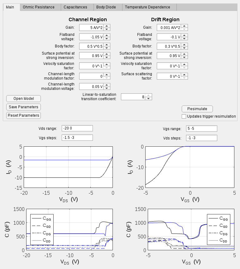
You can plot the basic I-V characteristics of the P-Channel LDMOS FET block without building a complete model. Use the plots to explore the impact of your parameter choices on device characteristics. If you parameterize the block from a data sheet, you can compare your plots to the data sheet to check that you parameterized the block correctly. If you have a complete working model but do not know which manufactured part to use, you can compare your plots to data sheets to help you decide.
To plot the basic I-V characteristics, set the Modeling option
parameter to No thermal port and, in the
Utilities section, click the
Plot button next to the Basic
characteristics parameter. (since R2026a) For more information about the
Basic characteristics parameter, see Plot Basic I-V Characteristics of Semiconductor Blocks.
Examples
Ports
Conserving
Parameters
References
[1] Aarts, A., N. D’Halleweyn, and R. Van Langevelde. “A Surface-Potential-Based High-Voltage Compact LDMOS Transistor Model.” IEEE Transactions on Electron Devices. 52(5):999 - 1007. June 2005.
[2] Van Langevelde, R., A. J. Scholten, and D. B. M. Klaassen. "Physical Background of MOS Model 11. Level 1101." Nat.Lab. Unclassified Report 2003/00239. April 2003.
[3] Oh, S-Y., D. E. Ward, and R. W. Dutton. “Transient analysis of MOS transistors.” IEEE J. Solid State Circuits. SC-15, pp. 636-643, 1980.

