Thyristor-Based Static Var Compensator
Introduction
The example described in this section illustrates application of Simscape™ Electrical™ Specialized Power Systems software to study the steady-state and dynamic performance of a static var compensator (SVC) on a transmission system. The SVC is a shunt device of the Flexible AC Transmission Systems (FACTS) family using power electronics. It regulates voltage by generating or absorbing reactive power.
Due to low frequencies of electromechanical oscillations in large power systems (typically 0.02 Hz to 2 Hz), this type of study usually requires simulation times of 30–40 seconds or more.
The SVC model described in this example is rather a detailed model of a particular SVC topology (using thyristor-controlled reactor (TCR) and thyristor-switched capacitors (TSCs)) with full representation of power electronics. This type of model requires discrete simulation at fixed time steps (50 µs in this case) and it is used typically for studying the SVC performance on a much smaller time range (a few seconds). Typical applications include optimizing of the control system, impact of harmonics, transients and stresses on power components during faults.
Description of the SVC
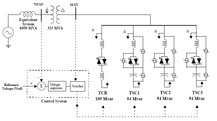
The single-line diagram of the modeled SVC is shown on Single-Line Diagram of the SVC. It represents a 300 Mvar SVC connected on a 735 kV transmission system.
This example is available in the Static Var Compensator (SVC) model. Load this model and save
it in your working directory as case2 to allow further
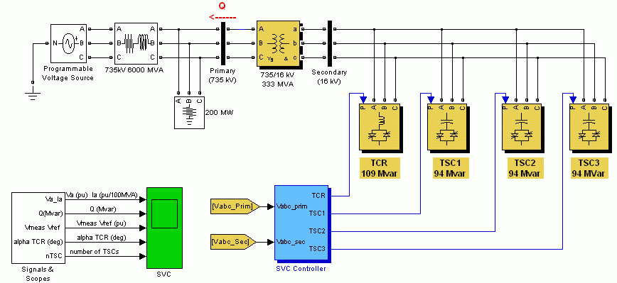
modifications to the original system. This model is shown on SPS Model of the 300 Mvar SVC on a 735 kV Power System (power_svc_1tcr3tscs).
Single-Line Diagram of the SVC

SPS Model of the 300 Mvar SVC on a 735 kV Power System (power_svc_1tcr3tscs)

SVC Power Components
The SVC consists of a 735 kV/16 kV, 333 MVA coupling transformer, one 109 Mvar TCR bank and three 94 Mvar TSC banks (TSC1 TSC2 TSC3) connected on the secondary side of the transformer.
Switching the TSCs in and out allows a discrete variation of the secondary reactive power from zero to 282 Mvar capacitive (at 16 kV) by steps of 94 Mvar, whereas phase control of the TCR allows a continuous variation from zero to 109 Mvar inductive. Taking into account the leakage reactance of the transformer (0.15 pu), the SVC equivalent susceptance seen from the primary side can be varied continuously from -1.04 pu/100 MVA (fully inductive) to +3.23 pu/100 Mvar (fully capacitive).
The SVC Controller monitors the primary voltage and sends appropriate pulses to the 24 thyristors (6 thyristors per three-phase bank) to obtain the susceptance required by the voltage regulator.
Each three-phase bank is connected in delta so that, during normal balanced operation, the zero-sequence tripplen harmonics (3rd, 9th,...) remain trapped inside the delta, thus reducing harmonic injection into the power system.
The power system is represented by an inductive equivalent (6000 MVA short circuit level) and a 200-MW load. The internal voltage of the equivalent system can be varied by means of a Three-Phase Programmable Voltage Source block to observe the SVC dynamic response to changes in system voltage.
SVC Control System
SVC Controller Model

The SVC control system consists of the following four main modules:
Measurement System measures the positive-sequence primary voltage. This system uses discrete Fourier computation technique to evaluate fundamental voltage over a one-cycle running average window. The voltage measurement unit is driven by a phase-locked loop (PLL) to take into account variations of system frequency.
Voltage Regulator uses a PI regulator to regulate primary voltage at the reference voltage (1.0 pu specified in the SVC Controller block menu). A voltage droop is incorporated in the voltage regulation to obtain a V-I characteristic with a slope (0.01 pu/100 MVA in this case). Therefore, when the SVC operating point changes from fully capacitive (+300 Mvar) to fully inductive (-100 Mvar) the SVC voltage varies between 1-0.03=0.97 pu and 1+0.01=1.01 pu.
Distribution Unit uses the primary susceptance Bsvc computed by the voltage regulator to determine the TCR firing angle α and the status (on/off) of the three TSC branches. The firing angle α as a function of the TCR susceptance BTCR is implemented by a look-up table from the equation
where BTCR is the TCR susceptance in pu of rated TCR reactive power (109 Mvar)
Firing Unit consists of three independent subsystems, one for each phase (AB, BC and CA). Each subsystem consists of a PLL synchronized on line-to-line secondary voltage and a pulse generator for each of the TCR and TSC branches. The pulse generator uses the firing angle α and the TSC status coming from the Distribution Unit to generate pulses. The firing of TSC branches can be synchronized (one pulse is sent at positive and negative thyristors at every cycle) or continuous. The synchronized firing mode is usually the preferred method because it reduces harmonics faster. Verify that the Synchronized firing mode has been selected in the Firing Unit dialog box.
Steady-State and Dynamic Performance of the SVC
Now observe the steady-state waveforms and the SVC dynamic response when the system voltage is varied. Run the simulation and observe waveforms on the SVC Scope block. These waveforms are reproduced below.
Waveforms Illustrating SVC Dynamic Response to System Voltage Steps

Initially the source voltage is set at 1.004 pu, resulting in a 1.0 pu voltage at SVC terminals when the SVC is out of service. As the reference voltage Vref is set to 1.0 pu, the SVC is initially floating (zero current). This operating point is obtained with TSC1 in service and TCR almost at full conduction (α = 96 degrees).
At t=0.1s voltage is suddenly increased to 1.025 pu. The SVC reacts by absorbing reactive power (Q=-95 Mvar) to bring the voltage back to 1.01 pu. The 95% settling time is approximately 135 ms. At this point all TSCs are out of service and the TCR is almost at full conduction (α = 94 degrees).
At t=0.4 s the source voltage is suddenly lowered to 0.93 pu. The SVC reacts by generating 256 Mvar of reactive power, thus increasing the voltage to 0.974 pu.
At this point the three TSCs are in service and the TCR absorbs approximately 40% of its nominal reactive power (α =120 degrees).
Observe on the last trace of the scope how the TSCs are sequentially switched on and off. Each time a TSC is switched on the TCR α angle changes from 180 degrees (no conduction) to 90 degrees (full conduction). Finally, at t=0.7 s the voltage is increased to 1.0 pu and the SVC reactive power is reduced to zero.
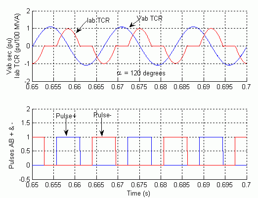
You may open the Signal & Scopes subsystem to observe additional waveforms. The TCR voltage and current in branch AB as well as thyristors pulses are displayed on the TCR AB scope. The figure below zooms on three cycles when the firing angle α is 120 degrees.
Steady-State Voltage and Current in TCR AB

Misfiring of TSC1
The final case study simulates a TSC misfiring.
Each time a TSC is switched off a voltage remains trapped across the TSC capacitors. If you look at the TSC1 Misfiring scope inside the Signals & Scope subsystem, you can observe the TSC1 voltage (first trace) and the TSC1 current (second trace) for branch AB. The voltage across the positive thyristor (thyristor conducting the positive current) is shown on the third trace and the pulses sent to this thyristor are shown on the fourth trace. Notice that the positive thyristor is fired at maximum negative TSC voltage, when the valve voltage is minimum.
If by mistake the firing pulse is not sent at the right time, very large overcurrents can be observed in the TSC valves. Look inside the SVC Controller block for how a misfiring can be simulated on TSC1. A Timer block and an OR block are used to add pulses to the normal pulses coming from the Firing Unit.
Open the Timer block menu and remove the 100 multiplication factor. The timer is now programmed to send a misfiring pulse lasting one sample time at time t= 0.121 s.
Restart simulation. Waveforms observed on the TSC1 Misfiring scope are reproduced below.
TSC Voltages and Current Resulting from Misfiring on TSC1

Observe that the misfiring pulse is sent when the valve voltage is maximum positive immediately after the TSC has blocked. This thyristor misfiring produces a large thyristor overcurrent (18 kA or 6.5 times the nominal peak current). Also, immediately after the thyristor has blocked, the thyristor voltage reaches 85 kV (3.8 times the nominal peak voltage). To prevent such overcurrents and overvoltages, thyristor valves are normally protected by metal oxide arresters (not simulated here).