Perform Large Matrix Operations Using External Memory
This example shows how to generate an HDL IP core with an AXI4 Master interface, perform matrix multiplication within the IP core, and store the output in external DDR memory.
Required Software and Hardware
To run this example, you must have the following software and hardware installed and set up:
Xilinx® Vivado® Design Suite, with supported version listed in HDL Language Support and Supported Third-Party Tools and Hardware.
Xilinx Zynq® ZC706 Evaluation Kit.
HDL Coder™ Support Package for Xilinx FPGA and SoC Devices.
HDL Verifier™ Support Package for Xilinx FPGA Boards.
You can also run this example on Xilinx Zynq Ultrascale+ MPSoC ZCU102 Evaluation Kit and Xilinx Versal™ AI Core Series VCK190 Evaluation Kit.
Overview of External Memory Workflow
In this example, you:
Generate an HDL IP core with AXI4 Master interface.
Access large matrices from the external DDR3 memory on the Xilinx Zynq ZC706 board using the AXI4 Master interface.
Perform matrix vector multiplication in the HDL IP core and write the output result back to the DDR memory using the AXI4 Master interface.
You can also run this example on a Xilinx Zynq Ultrascale+ MPSoC ZCU102 Evaluation Kit to access external DDR4 memory or on a Xilinx Versal AI Core Series VCK190 Evaluation Kit to access LPDDR4 memory.
This example models a matrix vector multiplication algorithm and implements the algorithm on the Xilinx Zynq FPGA board. Large matrices may not map efficiently to Block RAMs on the FPGA fabric. Instead, we can store the matrices in the external DDR memory on the FPGA board. The AXI4 Master interface accesses data through vendor-provided memory interface IP cores connected to DDR memory. This capability enables you to model algorithms that process large data and require high-throughput DDR access, such as matrix operations and computer vision algorithms.
The matrix-vector multiplication module supports fixed-point operations with a configurable matrix size ranging from 2 to 4000. The matrix size is configurable at run time through an AXI4-accessible register.
modelname = 'hdlcoder_external_memory';
open_system(modelname);

Designing Model with AXI4 Master Protocol
This example model includes the FPGA implementable DUT (Design under test) block, the DDR functional behavior block and the test environment to drive inputs and verify the expected outputs.
The DUT subsystem contains the AXI4 Master read/write controller and the matrix-vector multiplication module. Using the AXI4 Master interface, the DUT subsystem reads data from external DDR memory, feeds the data into the Matrix_Vector_Multiplication module, and writes the output back to DDR memory. The DUT module has several parameter ports mapped to AXI4-Lite-accessible registers. You can adjust these parameters from MATLAB®, even after implementing the design on the FPGA.
The DDR module represents external DDR memory in the simulation environment. The interface between the DUT and DDR modules uses the simplified AXI4 Master protocol.
The parameter port matrix_mul_on controls whether to run the Matrix_Vector_Multiplication module. When the input to matrix_mul_on is true, the DUT subsystem performs matrix vector multiplication as describe above. When the input to matrix_mul_on is false, the DUT subsystem perform a data loop back mode. In this mode, the DUT subsystem reads data from external DDR memory, writes it into the Internal_Memory module, and then writes the same data back to DDR memory. Data loopback mode provides a simple way to verify AXI4 Master external DDR memory access functionality.
open_system("hdlcoder_external_memory/DUT");

Inside the DUT subsystem, the DDR_Access module models the simplified AXI4 Master protocol, and use it to read and writes data on DDR. During IP Core Generation, HDL Coder generates a translator between the simplified AXI4 Master protocol and the actual AXI4 Master protocol in the generated HDL IP core. For more information on the simplified AXI4 Master protocol, see Model Design for AXI4 Master Interface Generation.
The Matrix_Vector_Multiplication module uses a multiply-add block to implement a streaming dot-product computation for the inner product of the matrix-vector multiplication.
Lets say, A be a matrix of size NxN and B is a vector of size Nx1.
Then, matrix vector multiplication output will be: Z = A * |B|, of size Nx1.
The first N values from the DDR are treated as the Nx1 size vector, followed by NxN size matrix data. First N values (vector data) are stored into a RAM. From N+1 values onwards, data is directly streamed as matrix data. Vector data will be read from the Vector_RAM in parallel. Both matrix and vector inputs are fed into the Matrix_mul_top subsystem. The first matrix output is available after N clock cycles and will be stored into output RAM. Again, vector RAM read address is reinitialized to 0 and starts reading same vector data corresponding to new matrix stream. This operation repeats for all rows of the matrix.
This diagram shows the architecture of the Matrix_Vector_Multiplication module.

Simulate and Verify External Memory Model in Simulink
You can simulate this hdlcoder_external_memory model, and verify the simulation result by running following script in MATLAB:
hdlcoder_external_memory_simulation;
PASSED: DDR initialization data matches.
PASSED: Matrix vector multiplication output matches with the expected data
Similarly, if you are targeting this example on the Xilinx Versal AI Core Series VCK190 Evaluation Kit, you can verify the simulation results by running the following script for hdlcoder_external_memory_64bit model.
hdlcoder_external_memory_64bit_simulation
The script initializes parameters such as Matrix_Size. By default, Matrix_Size is 64 (a 64*64 matrix) to keep simulation fast. After implementing the DUT on the FPGA board, you can use a larger Matrix_Size because FPGA computation is much faster.
The script then simulates the model, and verifies the result by comparing the logged simulation result with the expected value.
By default, the Matrix_Multiplication_On is true, the script verifies the matrix vector multiplication result.
When Matrix_Multiplication_On is false, the script verifies loopback mode. In this mode, the DUT reads Burst_Length data from DDR and writes it back to DDR.
If you have a DSP System Toolbox™ license, use Logic Analyzer to view model signals over time.

Generate HDL IP core for AXI4 Master interface.
Start the HDL Workflow Advisor and use the IP Core Generation workflow to deploy this design on Zynq hardware. For a detailed step-by-step guide, see Get Started with IP Core Generation from Simulink Model.
1. Set up the Xilinx Vivado synthesis tool path using the following command in the MATLAB command window. Use your own Vivado installation path when you run the command.
hdlsetuptoolpath('ToolName', 'Xilinx Vivado', 'ToolPath', 'C:\Xilinx\Vivado\2023.1\bin\vivado.bat')
2. Start the HDL Workflow Advisor from the DUT subsystem, hdlcoder_external_memory/DUT. The target interface settings are saved on the model. Notice that Target workflow is IP Core Generation, Target platform is Xilinx Zynq ZC706 evaluation kit, Reference Design is Default System with External DDR3 memory access, and Target platform interface table settings are as shown below.

In this example, input parameter ports such as matrix_mul_on, matrix_size, burst_len, burst_from_ddr, and burst start are mapped to the AXI4-Lite interface. HDL Coder generates AXI4-accessible registers for these ports. You can tune these parameters from MATLAB® at run time when the design runs on the FPGA board.
The AXI4 Master interface has separate read and write channels. Read channel ports (axim_rd_data, axim_rd_s2m, axim_rd_m2s) map to the AXI4 Master Read interface. Write channel ports (axim_wr_data, axim_wr_s2m, axim_wr_m2s) map to the AXI4 Master Write interface.
3. Right-click Task 3.2, Generate RTL Code and IP Core, and select Run to Selected Task to generate the IP core. Find register address mapping and documentation in the generated IP Core Report.
4. Now Right-click Task 4.2 Build FPGA Bitstream, and select Run to Selected Task to generate the Vivado project, and then build the FPGA bitstream.
During the project creation, the generated DUT IP core is integrated into the Default System with External DDR3 Memory Access reference design. This design includes a Xilinx Memory Interface Generator IP to communicate with on-board DDR3 memory on the ZC706 platform. An AXI Manager IP is also added to enable MATLAB® to control the DUT IP and initialize and verify DDR memory content.
Click the link in the Task 4.1 "Create Project" result window to view the generated Vivado project. Opening the Vivado block design shows a reference design similar to this architecture diagram.

Deploy and Validate FPGA Implementation on Zynq ZC706
After generating the FPGA bitstream, run Task 4.3 Program Target Device to program the FPGA board through the JTAG cable.
You can run the FPGA implementation and verify hardware results by running the following script in MATLAB:
hdlcoder_external_memory_hw_run
This script first initializes the Matrix_Size to 500, which means a 500x500 matrix. You can adjust the Matrix_Size up to 4000.
The script configures AXI4 Master read and write channel base addresses. These addresses define the base address from which the DUT reads and writes to external DDR memory. In this script, the DUT reads from base address 80000000 and writes to base address 81000000.
The AXI Manager feature initializes external DDR3 memory with input vector and matrix data and clears the output DDR memory location.
Start the DUT calculation by controlling AXI4-Lite-accessible registers. The DUT IP core reads input data from DDR memory, performs matrix-vector multiplication, and writes the result back to DDR memory.
Finally, read the output back to MATLAB and compare it with the expected value to verify hardware results.

Accessing External DDR4 Memory on Xilinx Zynq Ultrascale+ MPSoC ZCU102 Evaluation Kit
1. Use the hdlcoder_external_memory to access external DDR4 memory on ZCU102 using the HDL Coder IP core generation workflow.
2. Start the HDL Workflow Advisor from the DUT subsystem, hdlcoder_external_memory/DUT. In Task 1.1 Set Target platform as Xilinx Zynq Ultrascale+ MPSoC ZCU102 Evaluation Kit and in Task 1.2 set Reference Design as Default System with External DDR4 Memory Access.
3. Right-click Task 4.2 Build FPGA Bitstream, and select Run to Selected Task to generate the Vivado project, and build the FPGA bitstream.
4. You can run Task 4.3 Program Target Device to program the device and verify the hardware result by running following script in MATLAB:
hdlcoder_external_memory_hw_run_ZCU102
This script first initializes the Matrix_Size to 2000, which means a 2000x2000 matrix. In this script, the DUT is reading from base address '80000000', and write to base address '90000000'.
Finally, read the output back to MATLAB and compare it with the expected value to verify hardware results.

Accessing External LPDDR4 Memory on Xilinx Versal AI Core Series VCK190 Evaluation Kit
In this example, unlike the Xilinx Zynq® ZC706 Evaluation Kit and the Xilinx Zynq Ultrascale+ MPSoC ZCU102 Evaluation Kit, the Xilinx Versal™ AI Core Series VCK190 Evaluation Kit uses a different model, hdlcoder_external_memory_64bit, to access external LPDDR4 memory. The DUT IP core uses a 64-bit address width to access LPDDR4 with 8G locations through the AXI4 Master interface.
1. Use the hdlcoder_external_memory_64bit model to access external LPDDR4 memory on Versal VCK190 using HDL Coder IP core generation workflow.
2. Start the HDL Workflow Advisor from the DUT subsystem, hdlcoder_external_memory_64bit/DUT. In Task 1.1 Set Target platform as Xilinx Versal AI Core Series VCK190 Evaluation Kit and in Task 1.2 set Reference Design as Default System with External LPDDR4 Memory Access.
3. Right-click Task 4.2 Build FPGA Bitstream, and select Run to Selected Task to generate the Vivado project and build the FPGA bitstream.
4. You can run Task 4.3 Program Target Device to program the device and verify the hardware result by running following script in MATLAB:
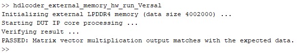
hdlcoder_external_memory_hw_run_Versal
This script first initializes the Matrix_Size to 2000, which means a 2000x2000 matrix. You can adjust the Matrix_Size up to 4000.
In this script, the DUT is reading from base address '50000000000', and write to base address '50100000000'.
Finally, read the output back to MATLAB and compare it with the expected value to verify hardware results.