DAC and ADC Data Loopback on RFSoC Device
This example shows how to capture raw analog-to-digital converter (ADC) data using the FPGA I/O API from the AMD® Zynq® UltraScale+™ RFSoC ZCU111, ZCU208, ZCU216, or DFE ZCU670 evaluation kit. This example uses the HDL Workflow Advisor to configure an SoC model for HDL code generation. In this example, you generate the HDL code for your algorithm, build and deploy the HDL design on an RFSoC device, and run a MATLAB® script to interactively capture data from the deployed HDL design.
Requirements
Vivado® Design Suite with a supported version listed in Supported EDA Tools and Hardware
Xilinx Zynq UltraScale+ RFSoC ZCU111, ZCU2028, ZCU216, or DFE ZCU670 evaluation kit
To set up the board connection for DAC and ADC loopback data capture, follow the hardware configuration settings for RFSoC boards in Board-Specific Setup Information.
Introduction
Open the example project and copy the example files to a temporary folder.
1. Navigate to the example source folder by entering these commands at the MATLAB command prompt.
example_root = (hdlcoder_rfsoc_examples_root)
cd (example_root)
Make sure that you have installed the HDL Coder Support Package for AMD FPGA and SoC Devices.
2. Copy all of the example files in the ADCDataCapture folder to a temporary folder.
This diagram depicts how the HDL design is used for this ADC capture example. The HDL Coder IP design transmits a numerically-controlled oscillator (NCO) waveform tone out of the digital-to-analog converter (DAC), which is then subsequently received by the ADC in the loopback configuration. AXI4-Stream transfers facilitate data movement back to the ARM processor in the Zynq RFSoC, which is then sent back to MATLAB over a TCP/IP connection.

Capture Logic Simulation
Simulate the model until the simulation terminates at the stop time. To examine the simulated captured data of the NCO waveform, open the DMA_Capture time scope plot, which this figure shows.
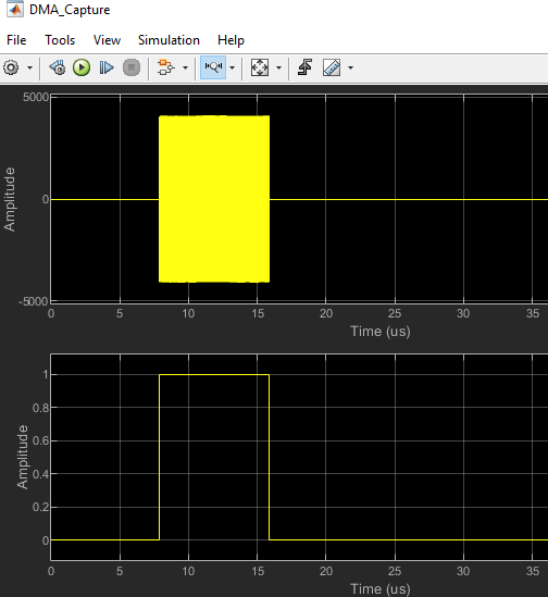
You can also view the captured data in MATLAB. The script rfsocADCCaptureSimulationPlot.m displays the data but uses the valid signal to extract the sample. This trimmed-down plot is what the direct memory access (DMA) transfers.

The simulation is set up such that the data movement logic moves 1024 samples of ADC samples when the trigger input is rising edge. This movement is done by using these two AXI4 register inputs.
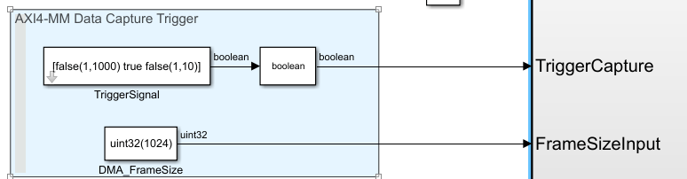
The register for the DMA frame size and the amount of data to transfer in the DMA must be equal. To examine the counter logic on how the capture is done, see this subsystem: rfsocADCCapture/ADC_Data_Capture/FrameCaptureValid.

Generate HDL and Synthesize Bitstream
If you are running the example on a Windows® platform, copy and paste the example into a new folder with a shorter path before running this example. There are path character-length limitations that cause Vivado to error. This issue is not present on Linux® platforms.
Open the model rfsocADCCapture.slx, and then right-click the ADC_Data_Capture subsystem. Select HDL Code, then click HDL Workflow Advisor.

Follow these steps in the HDL Workflow Advisor.
Step 1: Select Target Board
In step 1.1, select Target platform as Xilinx Zynq Ultrascale+ RFSoC ZCU111 Evaluation Kit, Xilinx Zynq Ultrascale+ RFSoC ZCU208 Evaluation Kit, Xilinx Zynq UltraScale+ RFSoC ZCU216 Evaluation Kit, or Xilinx Zynq UltraScale+ RFSoC DFE ZCU670 Evaluation Kit.
Right-click the design under test (DUT) subsystem, and then click Run This Task.
Step 2: Set Target Reference Design
In step 1.2, set Reference design to Real ADC/DAC Interface and the parameters in the Reference design parameters section to the indicated values in this figure.

These settings give an effective clock rate of 128 MHz for the HDL Coder generated IP core. This value is the result of using a decimation of 4x and four samples per clock at 2.048 giga samples per second (GSPS). This table provides the reference design parameters for the ZCU111 and ZCU216 boards. Before proceeding to the next step, set these reference design parameters to the indicated values.
AXI4-Stream Master data width to
64AXI4-Stream Slave data width to
64Add external memory access (AXI4 Master) to
falseADC sampling rate (MHz) to
2048ADC decimation mode (xN) to
4ADC samples per clock cycle to
4ADC mixer type to
BypassedDAC sampling rate (MHz) to
2048DAC interpolation mode (xN) to
4DAC samples per clock cycle to
4DAC mixer type to
BypassedADC/DAC NCO mixer LO (GHz) to
DisabledEnable multi-tile sync to
false
If you are using a ZCU208, ZCU216, or ZCU670 board, additionally set the DAC DUC mode parameter to Full DUC Nyquist (0-Fs/2).
Click Run This Task.
Step 3: Set Target Interface
The target interface settings are saved in the example model. In step 1.3, these target interface settings load automatically after you successfully run the Set Target Reference Design task.

If you are using a ZCU208 board, for the Tile1 DAC Ch3 Data port, set the target interface to Tile0 DAC Ch0 Data. For the Tile1 DAC Ch3 Valid port, set the target interface to Tile0 DAC Ch0 Valid.
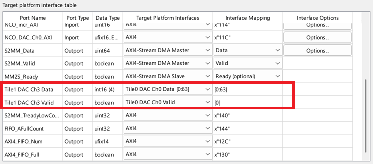
The port interface table designates the Simulink® subsystem input and outputs to an IP interface type. Options include AXI4-Stream DMA interfaces, ADC/DAC connections, and AXI4 slave registers. For more information on port interfacing, see Set Target Interface.
Step 4: Build FPGA Bitstream
To generate a Vivado project for synthesis and bitstream creation, see Build FPGA Bitstream. A command prompt window opens to display synthesis and place and route progress. Bitstream generation takes about 20 to 30 minutes to build depending on the specifications of your computer.

In step 4.2, to generate a script that provides MATLAB connectivity to the board for interactive testing and live I/O interfacing, select Generate host interface script and clear the Generate Simulink software interface model checkbox.
Program FPGA Bitstream
When the Vivado terminal reports that the FPGA bitstream has finished building, you can program the FPGA bitstream. Prior to programming the FPGA bitstream, you must ensure that the board has the correct SD card and is powered on. After Vivado programs the bit file, you see the message, which this figure shows.
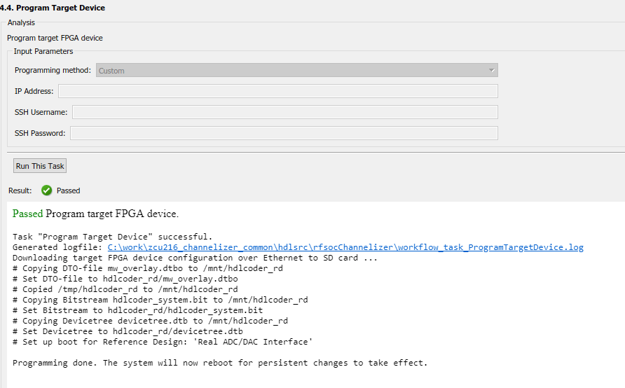
The board restarts and programs the bit file to the FPGA during initialization. On the next power or boot cycle, the board continues using this bitstream repeatedly until it is reprogrammed with a new bit file or until the SD card is reformatted. You do not need to repeatedly program the same bit file because it remains persistent until a new one needs to be loaded.
If you need to swap bitstreams for different designs, programmatically script this swap out rather than using the HDL Workflow Advisor again, which can be time consuming. You can use a script that can be generated in the workflow advisor.
Select File, then click Export to Script.

After the script is generated, edit the script to download the bitstream by setting the appropriate options to false, as this figure shows.

Set the last task, RunTaskProgramTargetDevice, to true.
Now, run this script to program the FPGA. If successful, the MATLAB output window displays a message indicating success.
You can reuse the preceding script for generating a Vivado project again. If you make a change in the Simulink HDL design, you must recompile the Vivado design.
ADC Data Capture
The HDL Coder Workflow Advisor generates scripts that you can use to help with communicating to the IP design deployed to the RFSoC at run time. These scripts include AXI4-Registers and AXI4-Streaming interfaces that are specified in the previous section in the workflow advisor. For more information, see the fpga object.
In this example, only the stream to memory-map (S2MM) interface is used to move data from the FPGA to the ARM processor by using the DMA. Several AXI4 registers are used to control the NCO tone, which transmits to the DAC.
The generated scripts are meant to be templates, which you can then customize to fit the intended application. To perform the data captures, this example provides MATLAB script files HostIO_rfsocADCCapture_setup.m and HostIO_rfsocADCCapture_interface.m. When the board is powered on after programming, the FPGA design runs the capture script. This script displays the ADC captured data plots.
HostIO_rfsocADCCapture_interface
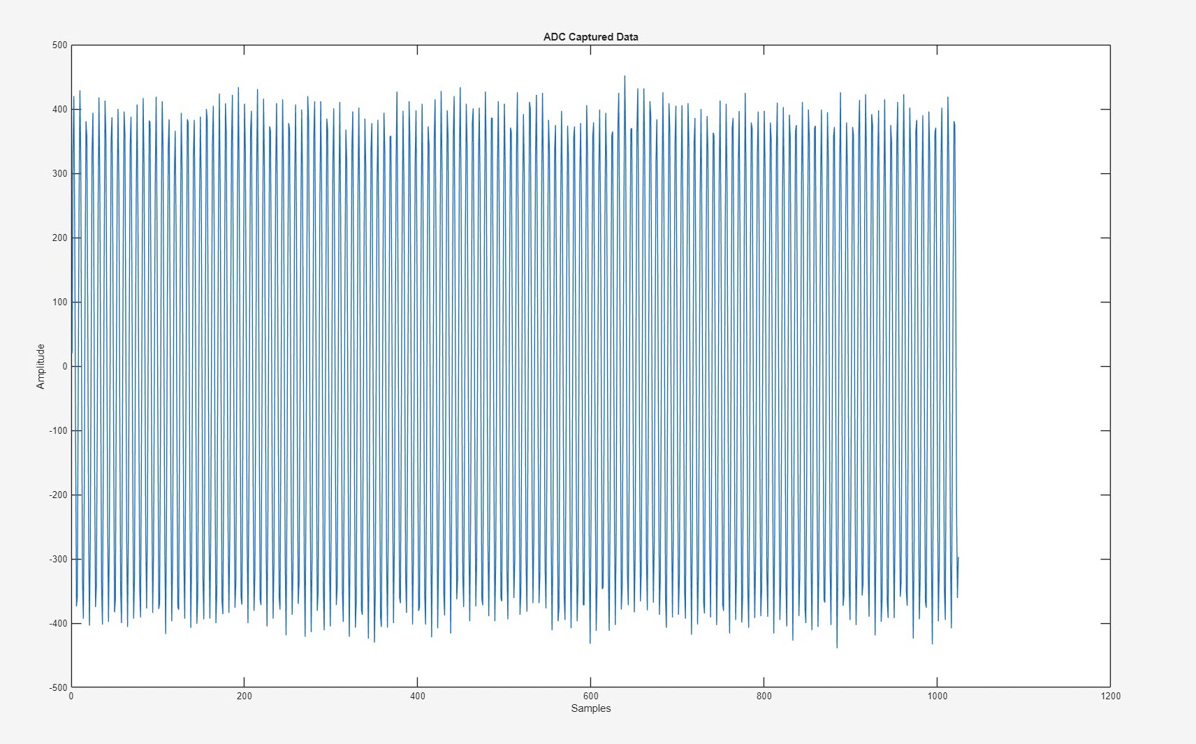
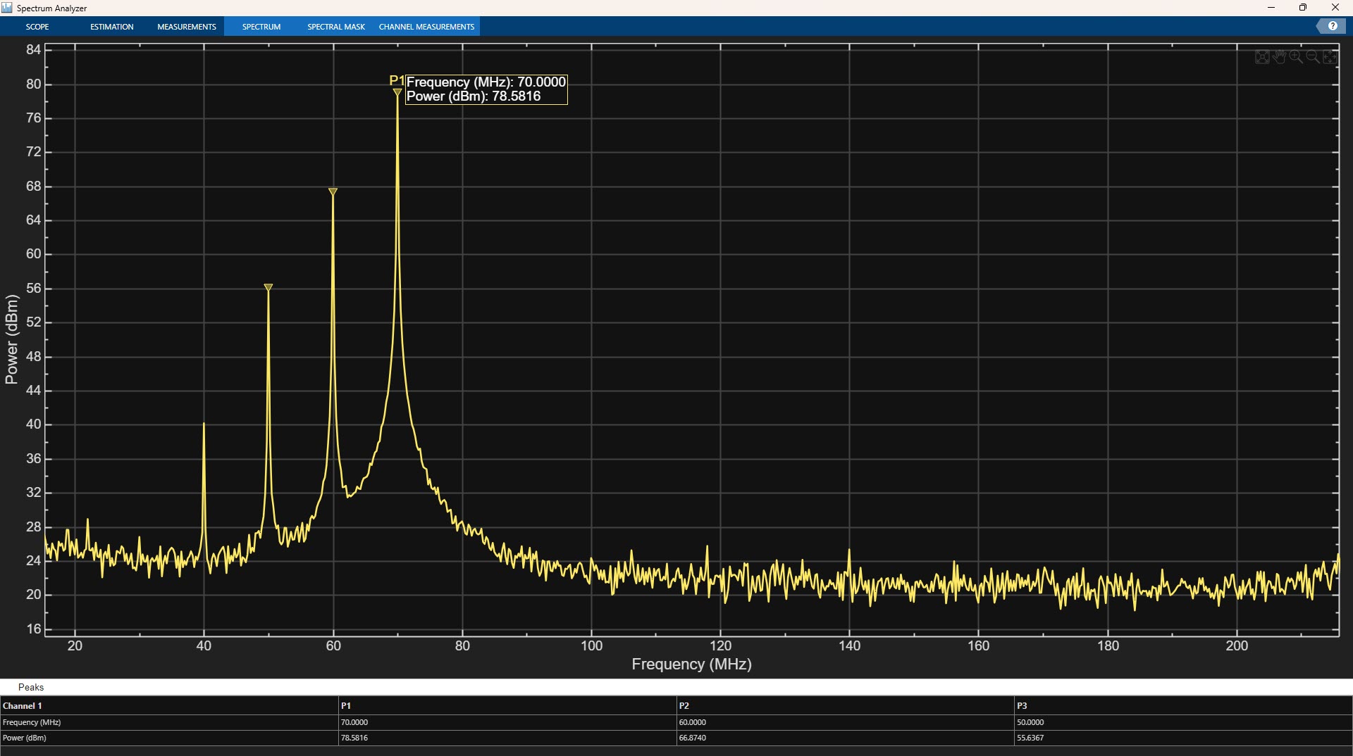
These time domain and spectrum plots show the resulting data captures. The script captures data in each iteration of a while loop while also changing the location of the NCO tone. To terminate the capture of data, close the ADC Captured Data figure. A register that is triggered by the software captures the data, and the rising edge detect logic that initiates data capture counters to move data into the AXI4-Stream S2MM.
Change Converter Settings
The RFSoC data converter contains settings and configuration options, some of which you can modify at run time. When the board is running and Linux starts, default settings are applied to the RF data converters that match the original design from the HDL Coder Workflow Advisor. This matching is accomplished with a CFG file that is uploaded to the board, and then read in during boot initialization.
To accommodate the modification of these parameters at run time, this example provides a programmatic MATLAB approach. Create the soc.RFDataConverter System object™ by using these commands in MATLAB.
rfobj = soc.RFDataConverter('ZU28DR','192.168.1.101'); % For ZCU111 board
rfobj = soc.RFDataConverter('ZU49DR','192.168.1.101'); % For ZCU216 board
This object requires the device and IP address as input arguments. Currently, RF data converter object supports these devices: ZU28DR (ZCU111) and ZU49DR (ZCU216). After creation, rfobj is an object in the MATLAB workspace. You can access this object further by using various object functions or properties to alter device settings.
This example provides a convenience script that gives an example of how to change the RF converter parameters. This script is autogenerated during the HDL Workflow Advisor workflow. In this ADC capture example, see the MATLAB script ADC_Data_Capture_setup_rfsoc.m.

If your system is connected to the board, then running this script shows the MATLAB prompt update with messages indicating that parameters are adjusted. For this example, the sampling rate is set for 2.048 GSPS with 4x interpolation and decimation for all ADC and DAC tiles. Because you can dynamically control the converter with this script, you can rerun the script with different values, such as changing the sampling rates or interpolation modes.
For example, if you change the decimator and interpolator to 8 instead of 4, your sampling rate is cut by half. You can transmit only the DAC NCO tone to 128 MHz (Fs as 1024 and Nyquist as Fs/2) rather than 256 MHz. This example also provides a log file that shows the TCP/IP activity between host and target for more details on what was sent back and forth.