Main Content

PCBWriter

Create PCB board definitions from 2-D antenna designs

Description

Use the PCBWriter object to create a printed circuit board (PCB) design files based on multilayer 2-D antenna design. A set of manufacturing files known as Gerber files describes a PCB antennas. A Gerber file uses an ASCII vector format for 2-D binary images.

Creation

Description

b = PCBWriter(pcbstackobject) creates a PCBWriter object that generates Gerber-format PCB design files based on a 2-D antenna design geometry using PCB stack.

example

b = PCBWriter(pcbstackobject,rfconnector) creates a customized PCB file using specified rfconnector type.

example

b = PCBWriter(pcbstackobject,writer) creates a customized PCB file using a specified PCB service, writer.

example

b = PCBWriter(pcbstackobject,rfconnector,writer) creates customised PCB file using specified PCB service and PCB connector type.

example

Input Arguments

expand all

Single feed PCB antenna, specified as a pcbStack object.

Example: p1 = pcbStack; a = PCBWriter(p1); creates a PCBWriter object from PCB stack.

Service to view PCB design, specified as a PCBServices object.

Example: s = PCBServices.MayhewWriter; a = PCBWriter(p1,s); uses Mayhew Labs PCB service to view the PCB design.

RF connector type for PCB antenna feedpoint, specified as a PCBConnectors object.

Example: c = PCBConnectors.SMA_Cinch; a = PCBWriter(p1,c); uses SMA_Cinch RF connector at feedpoint.

Output Arguments

expand all

PCB Board definition of 2.5D antenna design, returned as an object.

Properties

expand all

This property is read-only.

PCB Antenna geometry information, represented as a structure. The geometry information includes:

  • Layers — Vector of structures describing all metal layers.

  • FeedLocations — Cell vector defining antenna feed points.

  • ViaLocations — Cell vector specifying electrical connections (shorts) between pairs of metal layers in the antenna at specified locations.

  • ViaDiameter — Diameter of the electrical shorts.

  • DefaultConnector — Default RF connector to add to the PCB, when no connector is specified.

  • DesignInfo — Structure containing title, comment, and attribute text for the PCB design.

  • Source — Source of the PCB design.

Data Types: struct

PCB manufacturing service to view PCB design, specified as a PCBServices object.

Example: a = PCBWriter; a.Writer = PCBService.MayhewWriter; uses Mayhew Labs PCB service to view the PCB design.

RF connector type for PCB antenna feedpoint, specified as a PCBConnectors object.

Example: a = PCBWriter(pcbStack); a.Connector = PCBConnectors.SMA_Cinch; uses SMA_Cinch RF connector at the feedpoint.

Use default connector, specified as 0 or 1.

Example: a.UseDefaultConnector = 1, where a is a PCBWriter object.

Data Types: logical

Line widths drawn around components on silk screens, specified as a positive scalar in mils.

Example: a.ComponentBoundaryLineWidth = 10, where a is a PCBWriter object.

Data Types: double

Font size to label components on silk screen, specified as a positive scalar in points.

Example: a.ComponentNameFontSize = 12, where a is a PCBWriter object.

Data Types: double

Design information text font size added outside board profile, specified as a positive scalar.

Example: a.DesignInfoFontSize = 12, where a is a PCBWriter object.

Data Types: double

Font used for component name and design info, specified as a character vector.

Example: a.Font = 'TimesNewRoman', where a is a PCBWriter object.

Data Types: char | string

Copper free margin around board, specified as a positive scalar in meters.

Example: a.PCBMargin = 0.7e-3, where a is a PCBWriter object.

Data Types: double

Add solder mask to top and bottom of PCB, specified as 'both', 'top', 'bottom' or 'none'.

Example: a.SolderMask = 'top', where a is a PCBWriter object.

Data Types: char | string

Generate solder paste files as a part of PCB stack, specified as 1 or 0.

Example: a.SolderPaste = 0, where a is a PCBWriter object.

Data Types: logical

Enable or disable watermark signature, specified as a logical value. By default, the signature is enabled. Specify value as 0 to disable the signature.

Example: a.EnableSignature=0, where a is a PCBWriter object.

Data Types: logical

Enable or disable connector labels, specified as a logical value. By default, the connector label is enabled. Specify value as 0 to disable the connector label.

Example: a.EnableConnectorLabel=0, where a is a PCBWriter object.

Data Types: logical

Object Functions

gerberWriteGenerate Gerber files
openFolderOpen folder containing generated Gerber files in files browser
sendToExport generated Gerber Files to service provider

Examples

collapse all

Create a coplanar inverted-F antenna.

fco = invertedFcoplanar(Height=14e-3,GroundPlaneLength=100e-3,...
    GroundPlaneWidth=100e-3);

Create a pcbStack object.

p = pcbStack(fco);
figure
show(p)
title("Inverted-F PCB Antenna")

Figure contains an axes object. The axes object with title Inverted-F PCB Antenna, xlabel x (mm), ylabel y (mm) contains 3 objects of type patch, surface. These objects represent PEC, feed.

Generate a Gerber format design file using PCB Writer.

PW = PCBWriter(p)
PW = 
  PCBWriter with properties:

                        Design: [1×1 struct]
                        Writer: [1×1 Gerber.Writer]
                     Connector: []
           UseDefaultConnector: 1
    ComponentBoundaryLineWidth: 8
         ComponentNameFontSize: []
            DesignInfoFontSize: []
                          Font: 'Arial'
                     PCBMargin: 5.0000e-04
                    Soldermask: 'both'
                   Solderpaste: 1
               EnableSignature: 1
          EnableConnectorLabel: 1

   See info for details

Create a coplanar inverted-F antenna.

fco = invertedFcoplanar(Height=14e-3,GroundPlaneLength=100e-3,...
    GroundPlaneWidth=100e-3);

Create a pcbStack object.

p = pcbStack(fco);
figure
show(p)
title("Inverted-F PCB Antenna")

Figure contains an axes object. The axes object with title Inverted-F PCB Antenna, xlabel x (mm), ylabel y (mm) contains 3 objects of type patch, surface. These objects represent PEC, feed.

Create an SMA_Cinch connector using the PCBConnectors object.

c = PCBConnectors.SMA_Cinch
c = 
  SMA_Cinch with properties:

                    Type: 'SMA'
                     Mfg: 'Cinch'
                    Part: '142-0711-202'
              Annotation: 'SMA'
               Impedance: 50
               Datasheet: 'https://belfuse.com/resources/Johnson/drawings/dr-142-0711-202.pdf'
                Purchase: 'https://www.digikey.com/product-detail/en/cinch-connectivity-solutions-johnson/142-0711-202/J10154TR-ND/3587681'
               TotalSize: [0.0071 0.0071]
           GroundPadSize: [0.0024 0.0024]
       SignalPadDiameter: 0.0017
         PinHoleDiameter: 0.0013
           IsolationRing: 0.0041
    VerticalGroundStrips: 1

   Cinch 142-0711-202 (Example Purchase)

Create a PCB design file for the antenna with the connector.

PW = PCBWriter(p,c)
PW = 
  PCBWriter with properties:

                        Design: [1×1 struct]
                        Writer: [1×1 Gerber.Writer]
                     Connector: [1×1 PCBConnectors.SMA_Cinch]
           UseDefaultConnector: 0
    ComponentBoundaryLineWidth: 8
         ComponentNameFontSize: []
            DesignInfoFontSize: []
                          Font: 'Arial'
                     PCBMargin: 5.0000e-04
                    Soldermask: 'both'
                   Solderpaste: 1
               EnableSignature: 1
          EnableConnectorLabel: 1

   See info for details

Create a coplanar inverted-F antenna.

fco = invertedFcoplanar(Height=14e-3,GroundPlaneLength=100e-3,...
    GroundPlaneWidth=100e-3);

Create a pcbStack object.

p = pcbStack(fco);
figure
show(p)
title("Inverted-F PCB Antenna")

Figure contains an axes object. The axes object with title Inverted-F PCB Antenna, xlabel x (mm), ylabel y (mm) contains 3 objects of type patch, surface. These objects represent PEC, feed.

Use an Advanced Circuits Writer as a PCB manufacturing service.

s = PCBServices.AdvancedCircuitsWriter
s = 
  AdvancedCircuitsWriter with properties:

               BoardProfileFile: 'legend'
          BoardProfileLineWidth: 1
                 CoordPrecision: [2 6]
                     CoordUnits: 'in'
              CreateArchiveFile: 1
                 DefaultViaDiam: 3.0000e-04
             DrawArcsUsingLines: 0
                 ExtensionLevel: 1
                       Filename: 'untitled'
                          Files: {}
         IncludeRootFolderInZip: 0
                   PostWriteFcn: @(obj)sendTo(obj)
    SameExtensionForGerberFiles: 0
                    UseExcellon: 1

Create an antenna PCB design file using the above service.

PW = PCBWriter(p,s)
PW = 
  PCBWriter with properties:

                        Design: [1×1 struct]
                        Writer: [1×1 PCBServices.AdvancedCircuitsWriter]
                     Connector: []
           UseDefaultConnector: 1
    ComponentBoundaryLineWidth: 8
         ComponentNameFontSize: []
            DesignInfoFontSize: []
                          Font: 'Arial'
                     PCBMargin: 5.0000e-04
                    Soldermask: 'both'
                   Solderpaste: 1
               EnableSignature: 1
          EnableConnectorLabel: 1

   See info for details

Create a coplanar inverted F antenna.

fco = invertedFcoplanar(Height=14e-3,GroundPlaneLength=100e-3,...
                  GroundPlaneWidth=100e-3);

Use this antenna to create a pcbStack object.
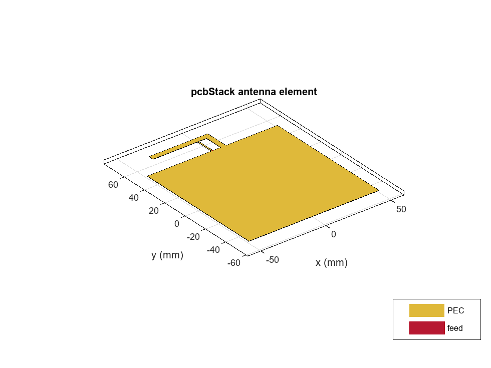
p = pcbStack(fco)
p = 
  pcbStack with properties:

              Name: 'Coplanar Inverted-F'
          Revision: 'v1.0'
        BoardShape: [1×1 antenna.Rectangle]
    BoardThickness: 0.0013
            Layers: {[1×1 antenna.Polygon]}
     FeedLocations: [0 0.0500 1]
      FeedDiameter: 5.0000e-04
      ViaLocations: []
       ViaDiameter: []
      FeedViaModel: 'strip'
       FeedVoltage: 1
         FeedPhase: 0
         Conductor: [1×1 metal]
              Tilt: 0
          TiltAxis: [1 0 0]
              Load: [1×1 lumpedElement]

figure
show(p)

Figure contains an axes object. The axes object with title pcbStack antenna element, xlabel x (mm), ylabel y (mm) contains 3 objects of type patch, surface. These objects represent PEC, feed.

Use an SMA_Cinch as an RF connector and Mayhew Writer as a 3-D viewer.

c = PCBConnectors.SMA_Cinch
c = 
  SMA_Cinch with properties:

                    Type: 'SMA'
                     Mfg: 'Cinch'
                    Part: '142-0711-202'
              Annotation: 'SMA'
               Impedance: 50
               Datasheet: 'https://belfuse.com/resources/Johnson/drawings/dr-142-0711-202.pdf'
                Purchase: 'https://www.digikey.com/product-detail/en/cinch-connectivity-solutions-johnson/142-0711-202/J10154TR-ND/3587681'
               TotalSize: [0.0071 0.0071]
           GroundPadSize: [0.0024 0.0024]
       SignalPadDiameter: 0.0017
         PinHoleDiameter: 0.0013
           IsolationRing: 0.0041
    VerticalGroundStrips: 1

   Cinch 142-0711-202 (Example Purchase)

s = PCBServices.MayhewWriter
s = 
  MayhewWriter with properties:

               BoardProfileFile: 'legend'
          BoardProfileLineWidth: 1
                 CoordPrecision: [2 6]
                     CoordUnits: 'in'
              CreateArchiveFile: 0
                 DefaultViaDiam: 3.0000e-04
             DrawArcsUsingLines: 1
                 ExtensionLevel: 1
                       Filename: 'untitled'
                          Files: {}
         IncludeRootFolderInZip: 0
                   PostWriteFcn: @(obj)sendTo(obj)
    SameExtensionForGerberFiles: 0
                    UseExcellon: 1

Create an antenna design file using PCBWriter.

PW = PCBWriter(p,s,c)
PW = 
  PCBWriter with properties:

                        Design: [1×1 struct]
                        Writer: [1×1 PCBServices.MayhewWriter]
                     Connector: [1×1 PCBConnectors.SMA_Cinch]
           UseDefaultConnector: 0
    ComponentBoundaryLineWidth: 8
         ComponentNameFontSize: []
            DesignInfoFontSize: []
                          Font: 'Arial'
                     PCBMargin: 5.0000e-04
                    Soldermask: 'both'
                   Solderpaste: 1

   See info for details

Use the gerberWrite function to generate gerber files from the antenna design files. Send the generated files to the Mayhew writer manufacturing service.

gerberWrite(PW)

The default folder containing the gerber files is named "untitled" and is located in your MATLAB folder. Running this example automatically opens up the Mayhew Labs PCB manufacturing service in your internet browser.

Drag and drop all your files from the "untitled" folder.

Click Done to view your Antenna PCB.

Version History

Introduced in R2017b

expand all