Systems Engineering Approach for SoC Applications
This example shows how to design a sample signal detector application on a System on Chip (SoC) platform using a systems engineering approach. The workflow in this example maps the application functions onto the selected hardware architecture.
The signal detector application continuously processes the signal data and classifies the signal as either high or low frequency. The signal cannot change between high- and low-frequency classes faster than 1 ms. The signal is sampled at the rate of 10 MHz.
Functional Architecture
Define the functional architecture of the application. At this stage, the implementation of the application components is not known. You can use the System Composer™ software to capture the functional architecture.
This model represents the functional architecture with its main software components and their connections.
systemcomposer.openModel('soc_signaldetector_func');
The functional architecture of the application consists of these top-level components:
Generate Signal
Preprocess Signal
Classify Signal
Activate LEDs
Hardware Architecture
Select the hardware architecture. Due to the anticipated application complexity, choose an SoC device. The chosen SoC device has a hardware programmable logic (FPGA) core and an embedded processor (ARM) core. You can use the System Composer software to capture the details of the hardware architecture.
This model represents the hardware architecture with its main hardware components and their connections.
systemcomposer.openModel('soc_signaldetector_arch');
Behavioral Modeling
If the implementations for functional components are available, you can add them to the functional architecture as behaviors. In System Composer, for each functional component, you can link the implementation behaviors as Simulink® models. To review the component implementations, double-click each component in the functional architecture model.
After you define the behavior of each component, you can simulate the behavior of the entire application and verify its functional correctness. Select Run in the functional architecture model. Then, analyze the signals classification results in the Simulation Data Inspector. To change the signal type, select the Generate Signal component and then select the Manual Switch block. Confirm that the source signal is classified correctly.
Allocation of Functional and Hardware Elements
After refining the functional and hardware architecture, allocate different functional components to different hardware elements to meet desired system performance benchmarks. In this case, some functional components are constrained as to where in the hardware architecture they can be implemented. You must implement the Generate Signal and Activate LEDs components on the FPGA core in the chosen hardware architecture due to input output (I/O) connections. Comparatively, you can implement the Preprocess Signal and Classify Signal components on either the FPGA or on the processor core.
               Component  Constraint
         Generate Signal        FPGA
       Preprocess Signal           -
         Classify Signal           -
           Activate LEDs        FPGA
This example shows how to use three possible scenarios for allocating the application functional architecture to the hardware architecture.
The FPGA handles preprocessing and classification.
The FPGA handles preprocessing and the processor handles classification.
The processor handles preprocessing and classification.
System Composer captures these scenarios as Scenario 1, Scenario 2, and Scenario 3 using the Allocation Editor (System Composer).
allocSet = systemcomposer.allocation.load('soc_signaldetector_allocation');
systemcomposer.allocation.editor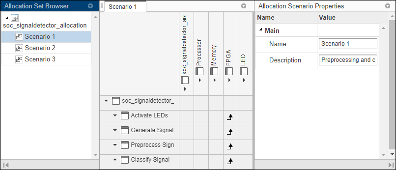
Choosing an allocation scenario requires finding an implementation that optimally meets the application requirements. Often you can find this implementation via static analysis without detailed simulation. In this example, use static analysis to analyze the computational costs of implementing different functional components on the processor and on the FPGA.
Implementation Cost
The implementation cost of a component depends on the required computation operations. To determine the implementation costs, consider these typical approaches.
Component implementation is not available: Obtain the computational cost from the available reference implementations.
The implementation and the hardware are available: Measure or profile the implementation cost on the candidate hardware.
The implementation is available, but the hardware is not: Estimate the implementation cost by using the SoC Blockset™ algorithm analyzer function
socAlgorithmAnalyzerReport.
The socModelAnalyzer function estimates the number of operations in a Simulink model and generates an algorithm analyzer report. To get the number of operations that a model executes to then analyze the implementation cost on the processor, use the dynamic analysis function option. To get the number of operators an algorithm requires to then analyze the implementation cost on the FPGA, use the static analysis function option. For an example on how to use socModelAnalyzer, see this sample function.
soc_signaldetector_costanalysis
*** Component: 'Preprocess Signal'
                                ADD(+)    MUL(*)
                                ______    ______

    FPGA Implementation            15        16
    Processor Implementation    15300     16320


*** Component: 'Classify Signal'
                                ADD(+)    MUL(*)
                                ______    ______

    FPGA Implementation            32        18
    Processor Implementation    32640     18360
The implementation costs for each functional component obtained in this code are entered in the corresponding stereotypes in the functional architecture. To verify the values, select each component in the functional architecture model and use the Property Inspector.
To learn more about socModelAnalyzer, see the Compare FIR Filter Implementations Using socModelAnalyzer example. This example shows how to analyze the computational complexity of different implementations of a Simulink algorithm.
Allocation Choice
You can use the number of operators or operations that are required for implementing the application functional components to decide how to allocate the functional components to the hardware components. Analyze the candidate allocations by comparing the implementation cost against the available resources of the FPGA and the processor. This example uses sample values in the FPGA and the processor components in the hardware architecture model for the available computation resources. Verify the values by using the Property Inspector.
Typically, the analysis does not use the number of operators or operations directly. Rather, the number of operators or operations are multiplied by the cost of each operator or operation first. The cost of the operator or operations is hardware dependent. Determining such costs is beyond the scope of this example.
For an example on how to use the cost models, use this function. Observe that we require the capacity of the FPGA and the processor be greater than the estimated implementation cost as well as that the processor headroom be between 60 and 90 %.
soc_signaldetector_partitionanalysis
                  FPGA DSPs Used (out of 900)    FPGA LUT Used (out of 218600)    Processor Instructions/s (out of 1000000000)    Processor Headroom (%)    Feasible
                  ___________________________    _____________________________    ____________________________________________    ______________________    ________

    Scenario 1                34                              576                                          0                               100                 0
    Scenario 2                16                              192                                  326400000                                67                 1
    Scenario 3                 0                                0                                  489600000                                51                 0
Based on the results Scenario 2 is feasible.
Data Path Design Between FPGA and Processor
The FPGA processes data sample-by-sample, and the processor processes frame-by-frame. Because the duration of a processor task can vary, to prevent data loss, a queue is needed to hold the data between the FPGA and processor. In this case you must set these parameters that are related to the queue: frame size, number of frame buffers, and FIFO size (that is, the number of samples in the FIFO). Also, in embedded applications, the task durations can vary between different task instances (for example, due to different code execution paths or due to variations in OS switching time). As a result, data might be dropped in the memory channel. The Streaming Data from Hardware to Software example shows a systematic approach to choosing the previously mentioned parameters that satisfy the application requirements.