Add Custom Board Definition for FPGA-in-the-Loop Using Gigabit Ethernet
This example shows how to support FPGA-in-the-loop (FIL) simulation on a custom FPGA board using Gigabit Ethernet. If HDL Verifier® does not support your FPGA board by default, create a custom board definition in the FPGA Board Manager. This example uses the AMD® Kintex™ 7 FPGA KC705 evaluation kit with the GMII Ethernet interface.
Requirements
See FPGA Board Requirements to verify that your board and Ethernet interface are supported for customization.
Before you begin, gather the following information:
Ethernet PHY connections and corresponding pin numbers
FPGA input clock frequency, clock type, pin number, and I/O standard
(Optional) Reset pin number, active level, and I/O standard
Find the details in the board specification provided by the vendor. For this example, see KC705 Evaluation Board for the Kintex-7 FPGA User Guide.
Create Board Definition
New FPGA Board Wizard
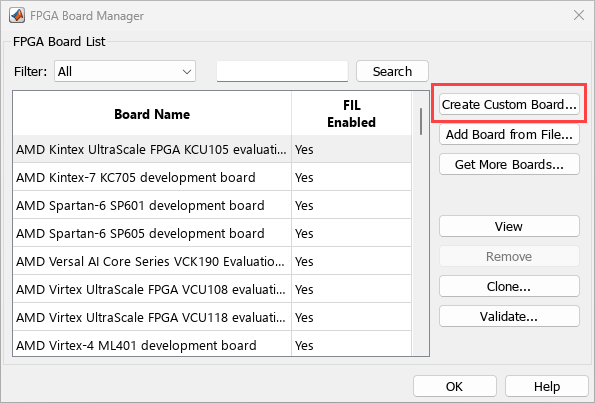
Open the FPGA Board Manager by entering the following command at the MATLAB® prompt:
fpgaBoardManager
Click Create Custom Board to open the New FPGA Board wizard.
Basic Information
In the Basic Information pane:
Set Board Name to
My AMD KC705 Board.Set Vendor to
AMD.Set Family to
Kintex7.Set Device to
xc7k325t.Set Package to
ffg900.Set Speed to
-2.Set JTAG Chain Position to
1. (This device is the only one in the JTAG chain.)
Click Next to continue.
Interfaces
In the Interfaces pane:
Select the FIL Interface check box.
Select Gigabit Ethernet - GMII for the PHY interface type.
Set Clock Frequency to
200. This board has multiple clock sources. The KC705 board supports multiple clock sources; 200 MHz is recommended for Ethernet interface.Set Clock Type to
Differential.Set Clock_P Pin Number to
AD12.Set Clock_N Pin Number to
AD11.Set Clock I/O Standard to
LVDS.Set Reset Pin Number to
AB7.Set Active Level to
Active-High.Set Reset I/O Standard to
LVCMOS15.
You can find these clock and reset details in the KC705 Evaluation Board for the Kintex-7 FPGA User Guide.
Click Next to continue.
FIL I/O
In the FIL I/O pane, enter the following values for each signal:
Signal Name | FPGA Pin Number | I/O Standard |
|---|---|---|
ETH_COL | W19 | LVCMOS25 |
ETH_CRS | R30 | LVCMOS25 |
ETH_GTXCLK | K30 | LVCMOS25 |
ETH_MDC | R23 | LVCMOS25 |
ETH_MDIO | J21 | LVCMOS25 |
ETH_RESET_n | L20 | LVCMOS25 |
ETH_RXCLK | U27 | LVCMOS25 |
ETH_RXD | U30,U25,T25,U28,R19,T27,T26,T28 | LVCMOS25 |
ETH_RXDV | R28 | LVCMOS25 |
ETH_RXER | V26 | LVCMOS25 |
ETH_TXD | N27,N25,M29,L28,J26,K26,L30,J28 | LVCMOS25 |
ETH_TXEN | M27 | LVCMOS25 |
ETH_TXER | N29 | LVCMOS25 |
For RXD and TXD, enter pin numbers from least significant bit (LSB) to most significant bit (MSB), separated by commas. These Ethernet PHY signal assignments are detailed in the KC705 Evaluation Board for the Kintex-7 FPGA User Guide.
The KC705 board uses a Marvell Alaska PHY (88E1111) for Ethernet communication at 10, 100, or 1000 Mb/s. It supports MII, GMII, RGMII, and SGMII interfaces between the FPGA and the PHY. The FPGA configures the PHY via the Management Data Input/Output (MDIO) bus, using PHY address 7 (binary 0b00111) for GMII mode.
To configure these settings, expand Advanced Options, select the Generate MDIO module to override PHY settings check box, and set the PHY address (0–31) to 7.
Click Next to continue.
Validation
You can validate your board customization by running an FPGA-in-the-loop (FIL) simulation test. To perform this validation, make sure that:
The AMD Vivado® tool is installed and on the MATLAB path. See AMD Usage Requirements for the recommended version.
The KC705 board is connected to your computer via an Ethernet cable.
To run this test:
Select the Run FPGA-in-the-Loop test check box and then select the Include FPGA board in the test check box.
If required, configure the IP address of the FPGA board and the network interface card (NIC) on your computer. For details, see Configure Network Interface Card (NIC) on Development Computer.
Click Run Selected Test(s). The test can take up to 30 minutes to complete.
Click Finish to exit the New FPGA Board wizard. When prompted, choose a location to save the FPGA board definition file and click Save. The new board now appears in the FPGA Board Manager. Click OK to close the FPGA Board Manager.
Run FIL Simulation on Custom Board
You can run the FIL simulation on the custom board by using either the FIL wizard or HDL Workflow Advisor.
Using FIL Wizard
Start the FIL wizard by entering the following command at the MATLAB prompt:
filWizard
Select My AMD KC705 Board from the Board Name list for FPGA-in-the-loop simulation.
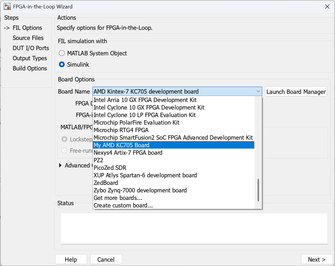
Then follow the steps to generate an FIL block or System object™ and run the FIL simulation. For example:
Using HDL Workflow Advisor
Start HDL Workflow Advisor from your Simulink® model or MATLAB code.
Set Target workflow to FPGA-in-the-Loop, and then select My AMD KC705 Board from the Target platform list for FPGA-in-the-loop simulation.
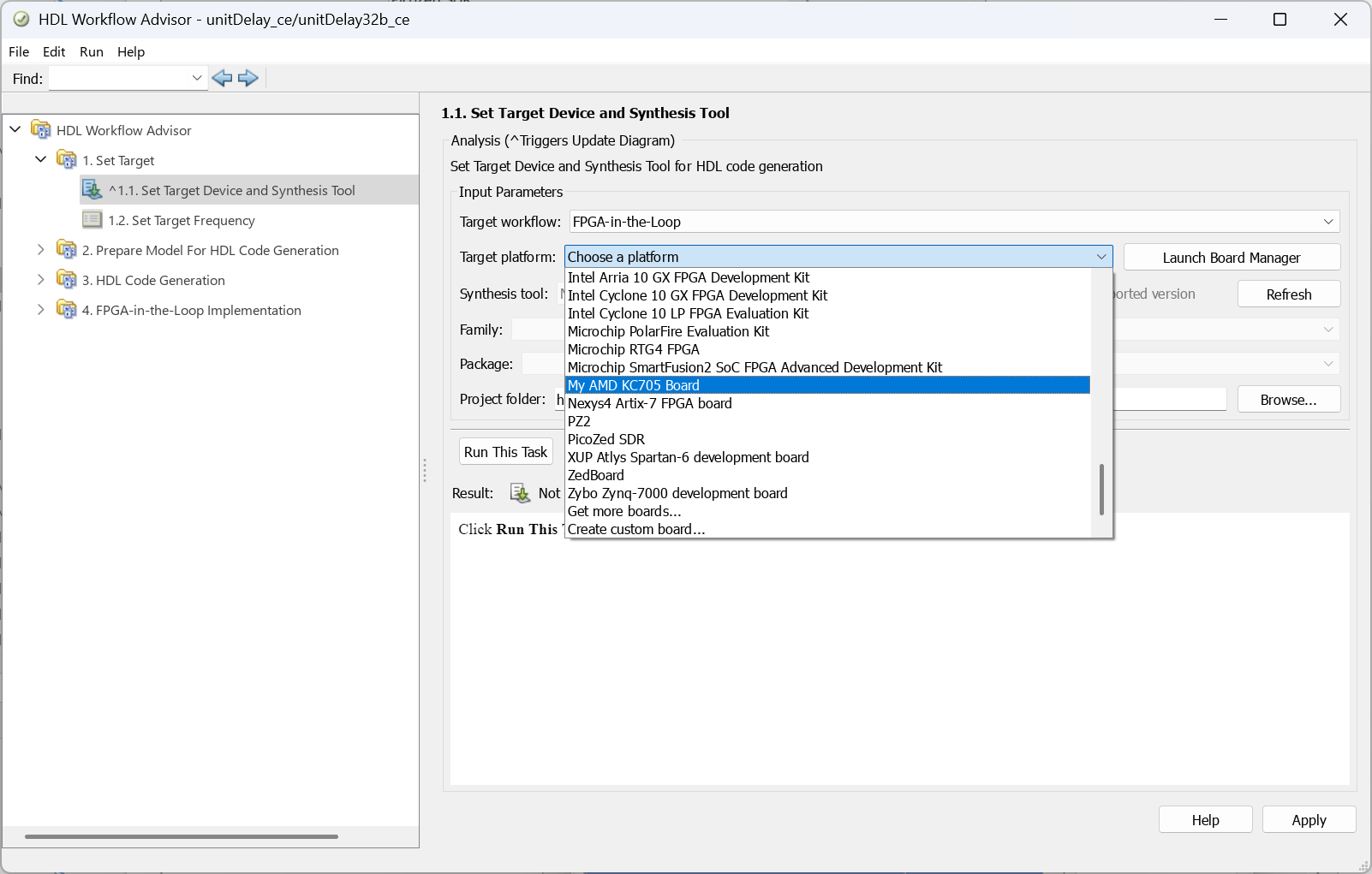
Then follow the steps to run the FIL simulation. For example: