Detect and Capture Wideband Radar Signal Using AMD RFSoC Device
This example shows how to build, simulate, and deploy a wideband radar signal detection and capture system in Simulink®. You use an SoC Blockset™ implementation and use it to target the AMD® Zynq® UltraScale+™ RFSoC evaluation kits. Using this example, you can detect radar signals over a 2 GHz bandwidth and capture the detected signals for further analysis. You partition the wideband radar signal detection and capturing functionality across the FPGA and the processor on the RFSoC device. The FPGA handles the wideband signal processing and the processor handles the system control, configuration, and status update. You also implement a radar emulator to generate pulsed radar signals and use these signals to evaluate the wideband detection and capturing capability of the system.
Supported Hardware Platforms
AMD Zynq UltraScale+ RFSoC ZCU111 evaluation kit with an XM500 balun card.
AMD Zynq UltraScale+ RFSoC ZCU216 evaluation kit with an XM655 balun card.
AMD Zynq UltraScale+ RFSoC ZCU208 evaluation kit with an XM655 balun card.
AMD Zynq UltraScale+ RFSoC DFE ZCU670 evaluation kit with an XM755 balun card.
Introduction
Radar signal detection is an important part of electronic warfare systems. Radar operators can detect radar emitters in the vicinity of key value installations and take appropriate countermeasures. In this example, you design a wideband radar signal detector system to detect and capture radar signals and identify the characteristics of the radar. The receiver monitors the entire spectrum of interest and identifies the narrowband channels containing valid signals. The receiver then captures the signals and transfers them to the host MATLAB® over FPGA I/O. You can then visualize and analyze the signals. The design also integrates a radar signal generator to transmit test signals for validating the signal detection functionality.
In this example, the design objective is to model the complete wideband radar system in a Simulink model and implement the system on an RFSoC device by using these generation workflows.
IP core generation workflow
SoC builder workflow
You can use either of these workflows to implement the wideband radar system. For more information about these workflows, see SoC Generation Workflows.
The system consists of a radar signal test transmitter, a wideband receiver, and a detector. The transmitter generates a train of linear frequency-modulated (LFM) pulses and transmits them through one of the DAC channels on the RFSoC device. You can configure the transmitter parameters during the design phase or after deployment. The receiver receives the radar signal and applies an energy detection algorithm to identify and extract the signal of interest. In this example, you pass the wideband input signal through a Channelizer to separate the individual channels of interest. You then identify the active channels using thresholding.
System Specifications
The system has these high-level specifications:
Receiver instantaneous bandwidth of 2 GHz
64 receiver channels
Receiver channel bandwidth of 30 MHz
This figure shows the implementation block diagram of the system.

IP Core Generation Workflow
For the IP core generation workflow, the example contains four different models.
hdl_radar_signal_detector_zcu111wideband radar signal detection on ZCU111 evaluation kit.hdl_radar_signal_detector_zcu216wideband radar signal detection on ZCU216 evaluation kit.hdl_radar_signal_detector_zcu208wideband radar signal detection on ZCU208 evaluation kit.hdl_radar_signal_detector_zcu670wideband radar signal detection on ZCU670 evaluation kit.
This example shows the workflow using the hdl_radar_signal_detector_zcu111 model. The workflow steps are common for all the four models.
open_system('hdl_radar_signal_detector_zcu111')

RF Data Converter Configuration
RFSoC devices have an RF Data Converter hardware IP connected to the programmable logic, which you configure according to your needs. Use the RF Data Converter block to configure the ADC and DAC settings of the AMD RF Data Converter IP and emulate the programmable logic interface to the converters.
To meet the system requirements of a 2 GHz of bandwidth, configure the RF Data Converter block by following these steps.
1. Choose the decimation factor and ADC sample rate based on the instantaneous bandwidth specification.
To achieve an instantaneous bandwidth of 2 GHz, set Sample rate (MSPS) to
4096. This value is the lowest sampling rate satisfying the Nyquist criterion that you can derive from the RF PLL reference on the ZCU111 board.
To achieve an instantaneous bandwidth of 2048 MHz, set the Decimation mode to
1and Interpolation mode to1.
2. Set Samples per clock cycle to 16 so that the FPGA clock rate is 256 MHz. The FPGA clock rate is the sampling rate divided by the product of the decimation factor and the number of samples per clock cycle, which in this case is equal to (4096/16) MHz, or 256 MHz.
3. To select specific ADCs and DACs, set RF Interface to Customize. To use the real interface, set the Digital interface to Real.
4. Select ADC 0 in ADC Tile 0 and DAC 2 in DAC Tile 1.
The ZCU111 evaluation board comes with an XM500 eight-channel SMA breakout card. This card has two ADC and two DAC single-ended channels (ADC224_T0_CH0, ADC224_T0_CH1, DAC229_T1_CH2, and DAC229_T1_CH3) for supporting a frequency range of 10 MHz to 1 GHz.

Hardware Logic Design
The top-level structure of the model includes four subsystems: Initialization, WidebandRadar, RF Data Converter, and Post Processing. The WidebandRadar subsystem in the design under test (DUT) generates HDL code. The other subsystems enable you to simulate the behavior of the DUT when deployed on the radio device.
The WidebandRadar subsystem contains two subsystems: Pulse Generator and Wideband Detector.
open_system('hdl_radar_signal_detector_zcu111/WidebandRadar')

close_system('hdl_radar_signal_detector_zcu111/WidebandRadar')
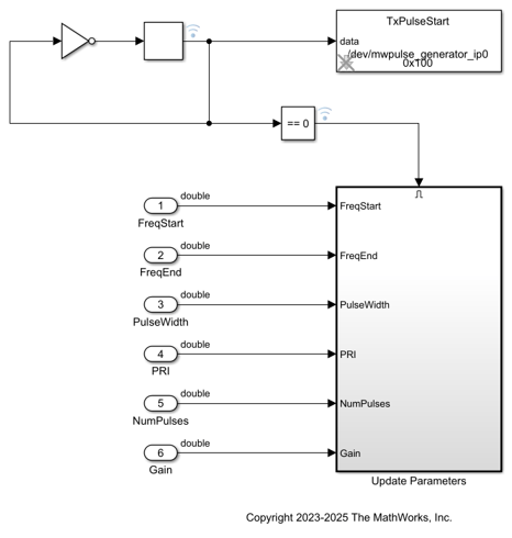
The Pulse Generator subsystem consists of the Pulse Generator Control and NCO LFM Generator subsystems. Use the Pulse Generator Control subsystem to define parameters that determine the timing of the signal generator, number of pulses, pulse repetition interval (PRI), and pulse width. You can configure these parameters at run time over an AXI4-Lite connection. The NCO LFM Generator subsystem then generates the linear FM waveform using a vector-based NCO. Use this subsystem to set parameters that determine the frequency characteristics of the waveform, such as the starting frequency and frequency step size.
The Wideband Detector subsystem implements the core receiver signal processing. The Channelizer block filters the wideband input signal from the ADC into the 64 narrowband channels. The Compute Power block then computes the power in each of the channels. The Detector block computes the moving average of the channel power levels and identifies that a signal is present when the current power is significantly greater than the moving average. When the block detects a signal, it selects the channel containing the highest power and provides the channel index to the subsequent processing blocks. The Output Capture block captures the channelized I/Q data from the channel containing the strongest signal. The To DMA Interface block sends the captured data packet to the processor.
The Initialization subsystem consists of all the parameters required to configure the DUT.
The Post Processing subsystem reads the data packet from the DUT and displays the detected signal.
Simulate Radar Detection System
To confirm the behavior of the model, simulate the system to visualize the detected signal and validate it against the characteristics of the transmitted radar waveform.

Generate IP Core
When you are satisfied with the simulated behavior of the model, you can proceed to integrate your design into a custom IP core by generating HDL code and mapping the model inputs and outputs to the hardware interfaces.
First, use the hdlsetuptoolpath (HDL Coder) function to set up the Xilinx® tool path. Specify the path to your Vivado® bin directory.
hdlsetuptoolpath('ToolName','Xilinx Vivado','ToolPath','/opt/Xilinx/Vivado/2024.1/bin');In the Simulink Toolstrip, from the Apps tab, select HDL Coder. In the HDL Code tab, follow these steps.
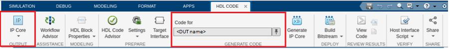
Make sure that the
WidebandRadarsubsystem is pinned in the Code for option. To pin this selection, select theWidebandRadarsubsystem in the Simulink model and click the pin icon.
Select IP Core as the Output > IP Core option.
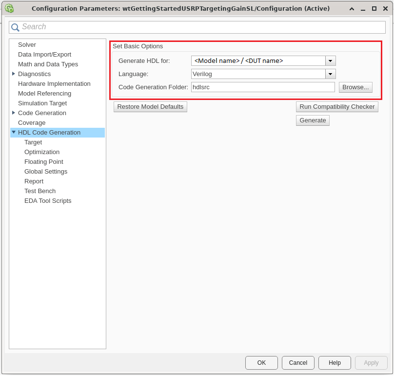
Configure HDL Code Generation
To open the Configuration Parameters window, in the HDL Code tab, click Settings. In the basic options of the HDL Code Generation panel, make sure that Language is set to VHDL or Verilog. By default, HDL Coder generates the VHDL or Verilog files in the hdlsrc folder. You can select an alternative location. If you make any changes, click Apply.
Configure HDL Code Generation Target
In the HDL Code Generation > Target > Workflow Settings, click Browse and select the project folder in which you want to save the generated project files.
In the HDL Code generation > Target > Reference Design Settings, set Reference Design to
Real ADC/DAC Interface. Set only AXI4-Stream Master data width and AXI4-Stream Slave data width to32. The RF Data Converter block connected within the Simulink model derives the remaining reference design settings.
Click Apply.
Configure Target Interface
1. In the HDL Code tab, click Target Interface to open the IP Core editor. 2. In the Interface Mapping tab, reload the port interface mapping options by clicking the Reload IP core settings and interface mapping table from model icon.

3. Validate the interface mapping by clicking the Validate IP core settings and interface mapping icon.
Generate the HDL code and IP core by clicking Generate IP Core.
Generate and Load Bitstream
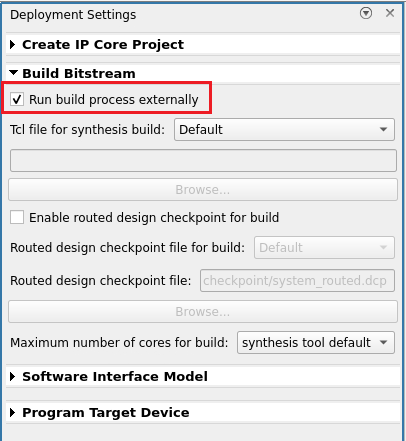
To generate a bitstream from the IP core, first open the deployment settings from the Build Bitstream dropdown and make sure that the Run build process externally option is selected. This setting is the default and ensures that the bitstream build executes in an external shell. The external shell allows you to continue using MATLAB while building the FPGA image.
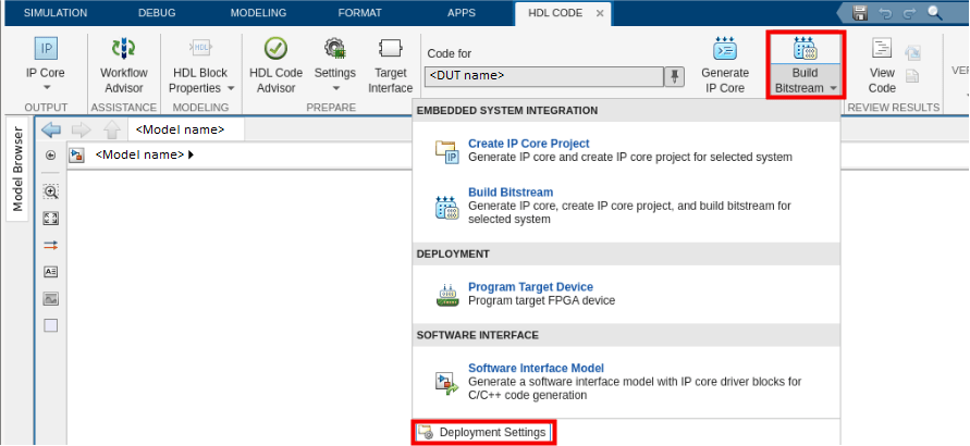
To create a Vivado IP core project and build the bitstream, click Build Bitstream. After the basic project checks complete, the Diagnostic Viewer displays a Build Bitstream Successful message along with warning messages. However, you must wait until the external shell displays a successful bitstream build before moving to the next step. Closing the external shell before this terminates the build. The bitstream for this project generates with the name system_wrapper.bit and is located in the vivado_ip_prj\vivado_prj.runs\impl_1 folder of the working directory after a successful bitstream build.
To load the bitstream onto the device, click Program Target Device from the Build Bitstream dropdown.
Alternatively, if you want to load the bitstream outside of this workflow, use the programFPGA function in the generated host interface script.
Generate Host Interface Script
In the HDL Code tab, Host Interface Script generates two MATLAB scripts, gs_hdl_radar_signal_detector_zcu111_interface.m and gs_hdl_radar_signal_detector_zcu111_setup.m, based on the target interface mapping you configured for your IP core.
The gs_hdl_radar_signal_detector_zcu111_interface.m script creates an fpga hardware object for interfacing with your FPGA from MATLAB. It contains MATLAB code that connects to your hardware and programs the FPGA.
The gs_hdl_radar_signal_detector_zcu111_setup.m script configures the fpga object with the hardware interfaces and ports from your DUT algorithm. It also contains DUT port objects that have the port name, direction, data type, and interface mapping information. It maps these DUT ports to the corresponding interfaces.
Use the generated host interface script as a starting point for deployment. Consider saving the generated script under a unique name and developing your algorithm there to read and write ports. The Host Interface Script button generates the scripts in your working directory.
Run Host Interface Script
Connect the SMA connectors on the XM500 Balun card to complete the loopback between the DAC and ADC channels, according to these connections and as shown in the figure.
DAC229_T1_CH2(J5) to ADC224_T0_CH0(J4).

For rapid prototyping, customize the host interface script based on your algorithm.
Modify the read and write commands in the interface script file to match your data requirements. Use the modified script with your deployed DUT IP core or algorithm running on the target board.
Run the sections of the host interface script to connect to your hardware board, program the FPGA, create an
fpgaobject, and set up the interfaces. The interfaces are set up based on the interface setup function file. You only need to run these sections once.Run the modified read and write commands and iterate on these commands.
When you have finished prototyping, release the connection to the hardware board.
This example uses an edited script based on the generated host interface script. Open the script for editing.
Open the hdl_radar_signal_detector_host_run_capture_io script.
Set the ZCU111 board IP address in the IPAddress field.
Run the script by clicking the Run button.
The script generates a plot containing the captured pulse in the time and frequency domains. The default value of the PRI is 50 microseconds. The pulse has a duration of 10 microseconds, a start frequency of 1305 MHz, and an end frequency of 1320 MHz. The estimated PRI, pulse duration, and pulse start and end frequencies must match the default settings.

SoC Builder Workflow
For the SoC builder workflow, the example contains four different top models.
soc_radar_signal_detector_zcu111_topwideband radar signal detection on ZCU111 evaluation kit.soc_radar_signal_detector_zcu216_topwideband radar signal detection on ZCU216 evaluation kit.soc_radar_signal_detector_zcu208_topwideband radar signal detection on ZCU208 evaluation kit.soc_radar_signal_detector_zcu670_topwideband radar signal detection on ZCU670 evaluation kit.
This example shows the workflow using the soc_radar_signal_detector_zcu111_top model. The workflow steps are common for all the four models.
Create the soc_radar_signal_detector_zcu111_top SoC model as the top model and set the hardware board to the Xilinx Zynq UltraScale+ RFSoC ZCU111 evaluation kit. This model includes the soc_radar_signal_detector_fpga FPGA model and the soc_radar_signal_detector_proc processor model as model references. The top model also includes an AXI4-Stream to Software block, which shares the external memory between the FPGA and the processor.
open_system('soc_radar_signal_detector_zcu111_top')

close_system('soc_radar_signal_detector_zcu111_top')
Hardware Logic Design
The RF data converter configuration and hardware logic design are the same as those in the IP core generation workflow model design.
open_system('soc_radar_signal_detector_fpga')

close_system('soc_radar_signal_detector_fpga')
Processor Logic Design
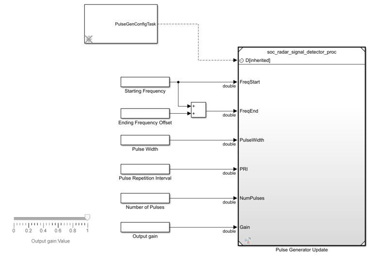
The soc_radar_signal_detector_proc processor model contains two subsystems: Pulse Generator Update and DMA Read Sim.
The Pulse Generator subsystem runs for every 0.2 seconds according to the PulseGenConfigTask defined in Task Manager block.
PulseGenConfigTask
Type of task - Timer.
Task period - 0.2 s.
Function - Control the timing execution of the software.
The DMA Read Sim subsystem reads the DMA packet from the FPGA and displays the detected signal.
open_system('soc_radar_signal_detector_proc')
close_system('soc_radar_signal_detector_proc')
Simulate Radar Detection System
Run the model to visualize the detected signal and validate it against the transmitted radar waveform characteristics.
Implement and Run Model on ZCU111 Hardware
To implement the model on a supported SoC board, use the SoC Builder tool. Set the Hardware Board to Xilinx Zynq UltraScale+ RFSoC ZCU111 Evaluation Kit on the System on Chip tab of the Simulink toolstrip.
To open SoC Builder, click Configure, Build, & Deploy. After the SoC Builder tool opens, follow these steps.
On the Setup screen, select Build model. Click Next.
On the Select Build Action screen, select Build and load for external mode. Click Next.
On the Select Project Folder screen, specify the project folder. Click Next.
On the Review Hardware Mapping screen, click Next.
On the Review Memory Map screen, to view the memory map, click View/Edit. Click Next.
On the Validate Model screen, to check the compatibility of the model for implementation, click Validate. Click Next.
On the Build Model screen, to build the model, click Build. An external shell opens when FPGA synthesis begins. Click Next.
On the Connect Hardware screen, to test the connectivity of the host computer with the SoC board, click Test Connection. To go to the Run Application screen, click Next.
The FPGA synthesis often takes more than 30 minutes to complete. To save time, you can use a pre-generated bitstream by following these steps.
Close the external shell to terminate the FPGA synthesis.
Copy the pre-generated bitstream to your project folder by entering this command at the MATLAB command prompt.
copyfile(fullfile(matlabshared.supportpkg.getSupportPackageRoot,
'toolbox','soc','supportpackages','xilinxsoc','xilinxsocexamples','bitstreams',
'soc_radar_signal_detector_zcu111_top-XilinxZynqUltraScale_RFSoCZCU111EvaluationKit.bit'),'./soc_prj');
Validate FPGA Design
Click Load and Run to load the pre-generated bitstream. You can use the automatically generated FPGA I/O script during the build process to quickly verify the FPGA algorithm. To validate the FPGA algorithm, load the bitstream and follow the same steps as in the IP core generation workflow.
Verify System in External Mode
You can now run the model in external mode or deploy the complete system, consisting of the processor and FPGA algorithms, onto hardware and verify the functionality.
After you load the bit file, close the generated software model and open the soc_radar_signal_detector_pulsegen_interface software model.
open_system('soc_radar_signal_detector_pulsegen_interface')
close_system('soc_radar_signal_detector_pulsegen_interface')
Run the model in external mode by clicking Monitor & Tune. After the model runs on hardware, run the soc_radar_signal_detector_host_run_capture_io script, ensuring that the hardware board IP address is correct. The detection information includes the detected radar PRI, as well as time and spectrum plots of the captured signal.
You can try updating the PRI, pulse duration, and pulse start and end frequencies with different values from the software model. You can then check whether the wideband detector detects the resultant characteristics and whether the hardware captures them adequately.
Implement and Run Model on ZCU216 Board
Configure Hardware
Connect the coarlisel and SMA connectors on the XM655 Balun card to complete the loopback between the DAC and ADC channels, according to the connections shown in the table.

IP Core Generation Workflow
Open the model by executing this command at the MATLAB command prompt.
open_system('hdl_radar_signal_detector_zcu216');To implement and run the model, follow the steps in the IP Core Generation Workflow section above for the ZCU111 board.
SoC Builder Workflow
Open the model by executing this command at the MATLAB command prompt.
open_system('soc_radar_signal_detector_zcu216_top');To implement and run the model, follow the steps in the SoC Builder Workflow section above for the ZCU111 board.
Implement and Run Model on ZCU208 Board
Configure Hardware
Connect the coarlisel and SMA connectors on the XM655 Balun card to complete the loopback between the DAC and ADC channels, according to the connections shown in the table.
IP Core Generation Workflow
Open the model by executing this command at the MATLAB command prompt.
open_system('hdl_radar_signal_detector_zcu208')To implement and run the model, follow the steps in the IP Core Generation Workflow section above for the ZCU111 board.
SoC Builder Workflow
Open the model by executing this command at the MATLAB command prompt.
open_system('soc_radar_signal_detector_zcu208_top')To implement and run the model, follow the steps in the SoC Builder Workflow section above for the ZCU111 board.
Implement and Run Model ZCU670 Board
Configure Hardware
Connect the coarlisel and SMA connectors on the XM755 Balun card to complete the loopback between the DAC and ADC channels, according to the connections shown in the table.
IP Core Generation Workflow
Open the model by executing this command at the MATLAB command prompt.
open_system('hdl_radar_signal_detector_zcu670')To implement and run the model, follow the steps in the IP Core Generation Workflow section above for the ZCU111 board.
SoC Builder Workflow
Open the model by executing this command at the MATLAB command prompt.
open_system('soc_radar_signal_detector_zcu670_top')To implement and run the model, follow the steps in the SoC Builder Workflow section above for the ZCU111 board.
Conclusion and Further Exploration
This example shows how to integrate a wideband radar signal detection system on an AMD RFSoC evaluation board using the IP core generation workflow and the SoC builder workflow. The example shows how to verify the design in a simulation and on hardware. The implementation detects a signal from a wideband channel, detects the characteristics, and captures the signal for further analysis.