FPGA Board Editor
To edit a board definition XML file, first make it writeable. If the file is read-only, the FPGA Board Editor only lets you view the board configuration information. You cannot modify that information.
General Tab
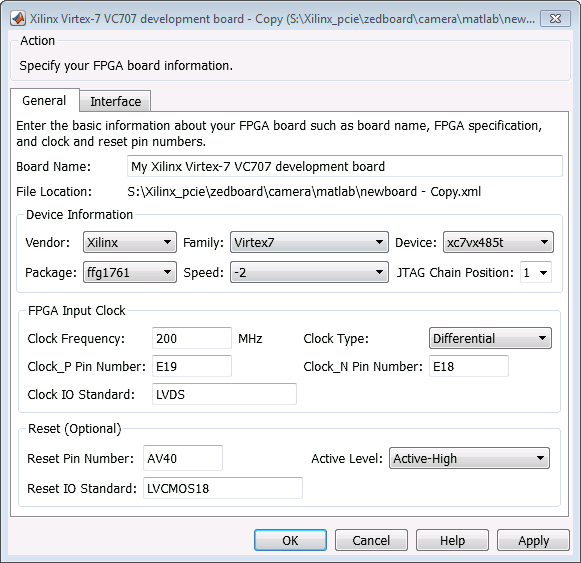
Board Name: Unique board name
Device Information:
Vendor:
AMDorAlteraFamily: Family depends on the specified vendor. See the board specification file for applicable settings.
Device: Device depends on the specified vendor and family. See the board specification file for applicable settings.
For AMD® boards only:
Package: Package depends on specified vendor, family, and device. See the board specification file for applicable settings.
Speed: Speed depends on package. See the board specification file for applicable settings.
JTAG Chain Position: Value indicates the starting position for JTAG chain. Consult the board specification file for this information.
FPGA Input Clock. Clock details are required for the FIL workflow. You can find all necessary information in the board specification file.
Clock Frequency. Must be from 5 through 300. For an Ethernet interface, the suggested clock frequencies are 50, 100, 125, and 200 MHz.
Clock Type:
Single_EndedorDifferential.Clock Pin Number (Single_Ended) — Must be specified. Example:
N10.Clock_P Pin Number (Differential) — Must be specified. Example:
E19.Clock_N Pin Number (Differential) — Must be specified. Example:
E18.Clock IO Standard — The programmable I/O Standard to use to configure input, output, or bi-directional ports. For example,
LVDS.
Reset (Optional). If you want to indicate a reset, find the pin number and active level in the board specification file, and enter that information.
Reset Pin Number. Leave empty if you do not have one.
Active Level :
Active-LoworActive-High.Reset IO Standard — The programmable I/O Standard to use to configure input, output, or bi-directional ports. For example,
LVCMOS33.
Interface Tab

The Interface page describes the supported FPGA I/O Interfaces. Select any listed interface and click View to see the Signal List. If the board definition file has write permission, you can also Add New interface, Edit the interface, or Remove an interface.
JTAG with Digilent Cable Setup
Note
Enter information for the JTAG cable setup carefully. If the settings are incorrect, the simulation errors out and does not work. If you are still unsure about how to setup your JTAG cable after reading these instructions, contact MathWorks® technical support with detailed information about your board.
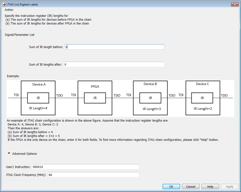
Signal/Parameter List — Provide the sum of the lengths of the instruction registers (IR) for all devices before and after the FPGA in the chain.
If the FPGA is the only item in the device chain, use zeros in both Sum of IR length before and Sum of IR length after.
If you are using a Zynq® device, and it is the only item in the device chain, set the Sum of IR length before and Sum of IR length after fields based on the JTAG chain position:
If the JTAG chain position is 1 (for example, the Zynq UltraScale+™ family), enter
0in Sum of IR length before and4in Sum of IR length after.If the JTAG chain position is 2 (for example, the Zynq-7000 family), enter
4in Sum of IR length before and0in Sum of IR length after.
If your board does not meet either of those conditions, follow these instructions to obtain the IR lengths:
Connect the FPGA board to your computer using the JTAG cable. Turn on the board.
Make sure that you installed the cable drivers during Vivado® installation.
Open Vivado Hardware Manager and select Open a new hardware target. In the dialog box is a summary of the IR lengths for all devices for that target.
Sum the IR lengths before the FPGA and enter the total in Sum of IR length before. Sum the IR lengths after the FPGA and enter the total in Sum of IR length after.
Vivado Hardware Manager cannot recognize the IR length of less common devices. For these devices, consult the device manual for instruction register length.
Advanced Options — If the default values are not the same as the most common settings for many devices, set the User1 Instruction and JTAG Clock Frequency (MHz) parameters. The most common settings are
000010and66, respectively.User1 Instruction — The JTAG USER1 Instruction defined in the AMD Bscane2 primitive. This binary instruction number, defined by AMD, varies from device to device. For most of the 7-series devices, this instruction is
000010. If your device has a different value, enter it in this parameter.To find this value, look at the
bsdfile for your specific device, found in your Vivado installation. For example, for the XA7A32T-CPG236 device, thebsdfile is located inVivado\2020.2\data\parts\xilinx\artix7\public\bsdl\xc7a35t_cpg236.bsd.Open this file. The
USER1value is000010. Enter this value at User1 Instruction."USER1 (000010),"
JTAG Clock Frequency (MHz) — Clock frequency used by the JTAG circuit. This value varies by device. You can find this value in the same
bsdfile described under User1 Instruction. For example, the JTAG clock frequency is 66 MHz for device XA7A32T-CPG236:attribute TAP_SCAN_CLOCK of TCK : signal is (66.0e6, BOTH);