CDSP Peripheral Configuration
Description
Add-On Required: This feature requires the Embedded Coder Support Package for Infineon AURIX TC4x Microcontrollers add-on.
Use the Hardware Mapping tool to view and edit the CDSP peripheral configuration parameters in Infineon® AURIX™ TC4x model.
Using the Hardware Mapping tool, you can:
View and edit configuration parameters for CDSP block.
Check for any conflicts between the peripherals.
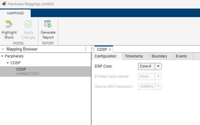
Open the CDSP Peripheral Configuration
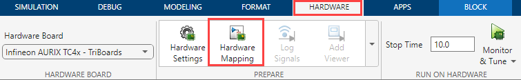
In the Hardware tab of the Simulink® model, click Model Settings to open the Configuration Parameters dialog box. Click on Hardware Implementation in the left pane and set Hardware board parameter to
Infineon AURIX TC4x - TriBoards.In the Hardware tab of the Simulink model, click Hardware Mapping. In the Mapping Browser pane, navigate to Peripherals > CDSP and select the tab for the peripheral parameters that you want to view and edit.
Parameters
Configuration
Select the primary input source of data on which the CDSP block performs different signal processing techniques.
This parameter must match the block or GP input registers connected to the Primary input port of the CDSP block in the Simulink model.
Note
If you set the DSP Filter chain parameter to
Demo FIR (FC0),Advanced average 1 (FC1),Advanced median (FC3), orAdvanced average 2 (FC4), then the CDSP block expects a 16-bit primary input from the GP registers.If you set the DSP Filter chain parameter to
Basic data accumulation (FC2)orBasic AURIX (FCM), then the CDSP block expects a 32-bit primary input from the GP registers, where the upper 16 bits represent side band signals of the data accumulation (DA) filter block. These side band signals control the integration operation in the DA filter block, with 0x6000 for integrator start and reset and 0x4000 for integrator start.
Select the TMADC channel number from which the CDSP block receives primary input data.
Note
This parameter must match the read-only parameter Channel in the Channel N tab of the corresponding TMADC block in the Hardware Mapping tool.
Dependencies
To enable this parameter, set the Primary input source
parameter to TMADC.
Select the secondary input source of data for Math filter block.
This parameter must match with the block or GP register connected to the Secondary input port of the CDSP block in the Simulink model.
Note
If you set the DSP Filter chain parameter to
Demo FIR (FC0),Advanced average 1 (FC1),Advanced median (FC3), orAdvanced average 2 (FC4), then the CDSP block expects a 16-bit secondary input from the GP registers.If you set the DSP Filter chain parameter to
Basic data accumulation (FC2)orBasic AURIX (FCM), then the CDSP block expects a 32-bit secondary input from the GP registers, where the first 16 bits represent side band signals of the data accumulation (DA) filter block. These side band signals control the integration operation in DA filter block, with 0x6000 for integrator start and reset and 0x4000 for integrator start.
Dependencies
To enable this parameter, set the DSP Filter chain
block parameter to Advanced average 1 (FC1),
Basic data accumulation (FC2), or
Advanced average 2 (FC4). This choice adds a
Math tab in the CDSP block, where you must set the Math
operation parameter to Addition with CDSP secondary
input or subtraction with CDSP secondary
input.
Select the TMADC channel number from which the CDSP block receives secondary input data.
Note
This parameter must match the read-only parameter Channel in the Channel # tab of the corresponding TMADC block in the Hardware mapping tool.
Dependencies
To enable this parameter, set the Secondary input
source parameter to TMADC.
Timestamp
Specify the division factor for the clock frequency to use in analog-to-digital conversion (ADC).
Dependencies
To enable this parameter, select the Enable timestamp output parameter in the CDSP block in the Simulink model.
Specify the source of the gate signal to trigger the timestamp.
Note
You must configure the appropriate trigger from the PWM block with a rate
(1/initial clock frequency of PWM) that is greater than the conversion time
of the filtered data output. Calculate this conversion time as Size
of filtered data x clock cycles / FADC.
For the filter chain FC0 with analog to digital
conversion frequency (FADC) of 160
MHz, 128 filter taps, and a decimation rate of
1, it requires 249 clock cycles to
output correct filtered data.
Dependencies
To enable this parameter, select the Enable timestamp parameter in the CDSP block of the Simulink model.
Specify the hardware trigger for the timestamp.
Dependencies
To enable this parameter, select the Enable timestamp parameter in the CDSP block of the Simulink model.
Select the type of hardware trigger edge to trigger the timestamp.
Dependencies
To enable this parameter, select the Enable timestamp parameter in the CDSP block of the Simulink model.
Specify the gate trigger delay for the timestamp.
Dependencies
To enable this parameter, select the Enable timestamp parameter in the CDSP block of the Simulink model.
Boundary
Set the lower limit of the boundary band to check the result.
Set the upper limit of the boundary band to check the result.
Enable hysteresis to avoid metastable states and switching due to internal ground bounce.
Activate boundary flag based on the boundary band limits.
Dependencies
To enable this parameter, disable the Enable hysteresis on boundary flag parameter.
Service request based on the boundary mode.
Integrator Control
Specify the hardware trigger source for integration in the DA filter block.
Dependencies
To enable this parameter, set the DSP filter chain
parameter to Basic data accumulation (FC2) or
Basic AURIX (FCM) in the CDSP block of the
Simulink model.
Specify the hardware trigger for integration in the DA filter block.
Note
Configure the ADC trigger from the PWM block. The Module, Timer submodule, Timer unit, and Trigger Channel parameter values in PWM Peripheral Configuration must match the values of the Window gate source and Hardware trigger parameters.
If your application model uses two CDSP blocks with DSP filter chain parameter set to
Basic data accumulation (FC2)andBasic AURIX (FCM), ensure sufficient time interval between subsequent PWM triggers signals for both filters chains to complete their operations. Otherwise, the filter chain produces a zero output for the next trigger signal.
Dependencies
To enable this parameter, set the DSP filter chain
parameter to Basic data accumulation (FC2) or
Basic AURIX (FCM) in the CDSP block of the
Simulink model.
Specify the hardware trigger edge for integration in the DA filter block.
Dependencies
To enable this parameter, set the DSP filter chain
parameter to Basic data accumulation (FC2) or
Basic AURIX (FCM) in the CDSP block of the
Simulink model.
Specify the trigger delay for integration in the DA filter block.
Dependencies
To enable this parameter, set the DSP filter chain
parameter to Basic data accumulation (FC2) or
Basic AURIX (FCM) in the CDSP block of the
Simulink model.
Events > Result Interrupt
Select this parameter to enable a result interrupt.
Specify the interrupt condition for the filtered result.
Source of the gate signal to trigger the filtered result.
Note
Ensure that you have configured the appropriate trigger using the PWM block.
Specify the hardware trigger for the filtered result.
Specify the trigger delay for the filtered result.
Events > Timestamp
Select this parameter to enable the timestamp interrupt.
Dependencies
To enable this parameter, select the Enable timestamp parameter in the CDSP block of the Simulink model.
Version History
Introduced in R2024a
See Also
MATLAB Command
You clicked a link that corresponds to this MATLAB command:
Run the command by entering it in the MATLAB Command Window. Web browsers do not support MATLAB commands.
웹사이트 선택
번역된 콘텐츠를 보고 지역별 이벤트와 혜택을 살펴보려면 웹사이트를 선택하십시오. 현재 계신 지역에 따라 다음 웹사이트를 권장합니다:
또한 다음 목록에서 웹사이트를 선택하실 수도 있습니다.
사이트 성능 최적화 방법
최고의 사이트 성능을 위해 중국 사이트(중국어 또는 영어)를 선택하십시오. 현재 계신 지역에서는 다른 국가의 MathWorks 사이트 방문이 최적화되지 않았습니다.
미주
- América Latina (Español)
- Canada (English)
- United States (English)
유럽
- Belgium (English)
- Denmark (English)
- Deutschland (Deutsch)
- España (Español)
- Finland (English)
- France (Français)
- Ireland (English)
- Italia (Italiano)
- Luxembourg (English)
- Netherlands (English)
- Norway (English)
- Österreich (Deutsch)
- Portugal (English)
- Sweden (English)
- Switzerland
- United Kingdom (English)